CY3220LINBUS-RD Cypress Semiconductor Corp, CY3220LINBUS-RD Datasheet - Page 54
CY3220LINBUS-RD
Manufacturer Part Number
CY3220LINBUS-RD
Description
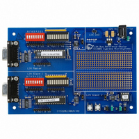
KIT REF DESIGN LIN BUS
Manufacturer
Cypress Semiconductor Corp
Series
PSoC®r
Datasheet
1.CY3220LINBUS-RD.pdf
(64 pages)
Specifications of CY3220LINBUS-RD
Main Purpose
Interface, LIN
Embedded
Yes, MCU, 8-Bit
Utilized Ic / Part
CY8C27143, CY8C27443
Processor To Be Evaluated
CY8C27143-24PXI and CY8C27443-24PXI
Interface Type
RS-232
Lead Free Status / RoHS Status
Contains lead / RoHS non-compliant
Lead Free Status / RoHS Status
Lead free / RoHS Compliant, Contains lead / RoHS non-compliant
Other names
428-1926


5. Demonstration Projects
5.4
5.4.1
Following are the functions performed by slave 1:
1. Initialize the hardware resources for resistance measurement, DIP switches and the LIN core.
2. Clear the Response_Error bit.
3. Inside an infinite Loop:
5.4.2
void main()
{
BYTE i;
52
❐
❐
❐
❐
// Initialize NAD
bLinNAD = 1;
// Initialize the LIN Interface
l_ifc_init();
// Initialize ports
PRT2DR = 0xFF;
PRT1DR = 0xFF;
bLED = 0x00;
// Initialize the status bytes of all the Frame buffers
BufferFrame1[0] = 0;
// BufferFrame2 carries the Response error bit.
// a flag in the buffers status byte to indicate that this
// frame carries the Response Error bit
BufferFrame2[0] = 0 | bfRESPONSE_ERROR_BYTE;
// Update the PreviousValue variable with PRT2DR status.
// write this value to the Data byte of Frame3 and set the
// DATA_READY flag so that data will be transmitted when this
// frame occurs the first time
PreviousValue = PRT2DR;
BufferFrame3[1] = PRT2DR;
BufferFrame3[0] = bfDATA_READY;
// Switch On REFLO RefMux and enable REFHI at the testMux of ACB00
ACB00CR2 &= 0xF3;
ACB00CR2 |= 0x1C;
// Start the REFLO mux
REFLO_Start(REFLO_MEDPOWER);
// Start the Input Buffer Amplifier
Buffer_Start(Buffer_MEDPOWER);
Check if Frame1 (VL1_CEM_Frm1) has completed successfully. If yes, update LED 1 to LED 8 with the switch status
sent by the master.
Measure the resistance function and update the buffer of Frame2 (VL1_CPM_Frm1) with resistance information and
also update the Response_Error bit.
Frame3 (VL1_CPM_Frm2) has been configured as an event-triggered frame. If there has been any change in the
SW1 and SW2 status, then update the buffer of Frame3. When the master initiates VL1_CPM_Frm2, the switch status
is transmitted as response.
Check if the GOTO_SLEEP flag has been set. If yes, enter the low-power mode.
Example Project for Slave 1 (CPM)
Description
Example Slave 1 Program
// Port2 reads the DIP switches
// Port1 drives the LEDs
Cypress Semiconductor – Rev. **
So set
Also
LIN Bus 2.0 Reference Design
October 25, 2006
Related parts for CY3220LINBUS-RD
Image
Part Number
Description
Manufacturer
Datasheet
Request
R

Part Number:
Description:
KIT DEMO PSOC CAPSENSE
Manufacturer:
Cypress Semiconductor Corp
Datasheet:

Part Number:
Description:
KIT DEMO PSOC CAPSENSE SLIDE
Manufacturer:
Cypress Semiconductor Corp

Part Number:
Description:
Manufacturer:
Cypress Semiconductor Corp
Datasheet:
Part Number:
Description:
Manufacturer:
Cypress Semiconductor Corp
Datasheet:
Part Number:
Description:
Manufacturer:
Cypress Semiconductor Corp
Datasheet:
Part Number:
Description:
Manufacturer:
Cypress Semiconductor Corp
Datasheet:
Part Number:
Description:
Manufacturer:
Cypress Semiconductor Corp
Datasheet: