CY3220LINBUS-RD Cypress Semiconductor Corp, CY3220LINBUS-RD Datasheet - Page 34
CY3220LINBUS-RD
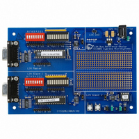
Manufacturer Part Number
CY3220LINBUS-RD
Description
KIT REF DESIGN LIN BUS
Manufacturer
Cypress Semiconductor Corp
Series
PSoC®r
Datasheet
1.CY3220LINBUS-RD.pdf
(64 pages)
Specifications of CY3220LINBUS-RD
Main Purpose
Interface, LIN
Embedded
Yes, MCU, 8-Bit
Utilized Ic / Part
CY8C27143, CY8C27443
Processor To Be Evaluated
CY8C27143-24PXI and CY8C27443-24PXI
Interface Type
RS-232
Lead Free Status / RoHS Status
Contains lead / RoHS non-compliant
Lead Free Status / RoHS Status
Lead free / RoHS Compliant, Contains lead / RoHS non-compliant
Other names
428-1926


4. Slave Design IP
all slaves are required to monitor the bus at all times in prep-
aration for the next message.
4.2
The LIN slave design has two configurations, the Synchro
Reception Configuration and the Data Reception Configura-
tion. The Synchro Reception Configuration detects the
break/synch signal and calculates the master’s bit rate. The
Data Reception Configuration receives the protected identi-
fier, decodes it and then either receives data from the mas-
ter or sends a response to the master.
4.2.1
Figure 4-1 shows the module placement for the Synchro
Reception Configuration. This configuration has one 16-bit
timer to find the timings between the rising and falling edges
of the break/synch signal and one 16-bit counter for timeout
operation. The RX pin is routed to the capture input of the
timer and configured to capture either rising edge or the fall-
ing edge of the input signal. Also, the GPIO interrupt is
enabled and all the calculations take place inside the GPIO
ISR.
Figure 4-1. Synchro Reception Configuration
4.2.2
Figure 4-2 shows the module placement for the Data Recep-
tion Configuration. This has one 8-bit counter that generates
the baud rate, one 8-bit counter that generates interrupts at
bit time to either detect timeouts while receiving data or to
check bit errors while transmitting data, one RX8 User Mod-
ule that receives data, and one TX8 User Module that trans-
mits data. The baud rate generator is configured according
to the bit rate calculated during the break/synch detection
stage. During data reception, the bit time counter generates
an interrupt every five bit times and a timeout counter is dec-
remented. If the frame is not completed within this timeout (if
the master stops transmitting), the Synchro Reception Con-
figuration is loaded. When transmitting, this timer generates
an interrupt every bit time. Inside the bit time counter ISR,
the states of TX and RX pins are compared. If they do not
match, then it is taken as a bit error and the transmission is
aborted and the Synchro Reception Configuration is
reloaded.
32
Device Configuration
Synchro Reception Configuration
Data Reception Configuration
Cypress Semiconductor – Rev. **
Figure 4-2. Data Reception Configuration
4.3
4.3.1
Once the foreground process calls the l_sys_init function
and starts the LIN firmware, all other operations take place
in the background inside ISRs. There are no blocking func-
tions in the LIN APIs, so that the main application runs in the
foreground. There are five different interrupts that are pro-
cessed inside the LIN firmware. Depending upon the active
state, some of these interrupts are active. The code inside
each of these ISRs is commented so that it is easy to under-
stand the operation. A brief description of each ISR is given
below.
4.3.2
This interrupt is active during the Synchro Reception Config-
uration. The break/synch field detection/decoding takes
place inside this ISR. This ISR is managed as a state
machine that has eight states.
A. Default State: Initially, when the Synchro Reception
B. Wait For Dominant Break: When the falling edge of the
C. Wait for Recessive Break: When the rising edge of the
D. Wait For Synchro Field: When the falling edge of the
Configuration is loaded, the GPIO interrupt is configured
to a falling edge interrupt and the timer capture is
enabled upon the falling edge of input. The state
machine is initialized to “Wait for Dominant Break.”
break signal is detected, this state is entered. Here, the
count latched to the compare register, due to the capture
of the timer, and is read into a temporary register. Then
the timer capture is configured to occur upon rising edge
of input. The GPIO is configured as a rising edge inter-
rupt. The state machine is initialized to “Wait for Reces-
sive Break.”
break signal is detected, this state is entered. Here, the
count latched to the compare register of the timer during
capture is read and the difference between this count
and the previously recorded count (during falling edge of
break) is found. This gives the time of the break field.
This value is stored in a variable to be processed later.
The timer is configured to capture upon falling edge and
the GPIO is configured as a falling edge interrupt. The
state machine is updated to “Wait for Synchro Field.”
start bit of the synchro field is detected, this state is
entered. Here, the compare register of the timer is read
Firmware
Overview
GPIO Interrupt
LIN Bus 2.0 Reference Design
October 25, 2006
Related parts for CY3220LINBUS-RD
Image
Part Number
Description
Manufacturer
Datasheet
Request
R

Part Number:
Description:
KIT DEMO PSOC CAPSENSE
Manufacturer:
Cypress Semiconductor Corp
Datasheet:

Part Number:
Description:
KIT DEMO PSOC CAPSENSE SLIDE
Manufacturer:
Cypress Semiconductor Corp

Part Number:
Description:
Manufacturer:
Cypress Semiconductor Corp
Datasheet:
Part Number:
Description:
Manufacturer:
Cypress Semiconductor Corp
Datasheet:
Part Number:
Description:
Manufacturer:
Cypress Semiconductor Corp
Datasheet:
Part Number:
Description:
Manufacturer:
Cypress Semiconductor Corp
Datasheet:
Part Number:
Description:
Manufacturer:
Cypress Semiconductor Corp
Datasheet: