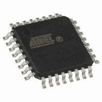
ATMEGA328P-AU Atmel, ATMEGA328P-AU Datasheet - Page 130

ATMEGA328P-AU
Manufacturer Part Number
ATMEGA328P-AU
Description
MCU AVR 32K FLASH 32TQFP
Manufacturer
Atmel
Series
AVR® ATmegar
Datasheets
1.ATMEGA48A-PU.pdf
(566 pages)
2.ATMEGA48A-PU.pdf
(33 pages)
3.ATMEGA48PA-MMH.pdf
(26 pages)
4.ATMEGA328P-AU.pdf
(567 pages)
Specifications of ATMEGA328P-AU
Core Processor
AVR
Core Size
8-Bit
Speed
20MHz
Connectivity
I²C, SPI, UART/USART
Peripherals
Brown-out Detect/Reset, POR, PWM, WDT
Number Of I /o
23
Program Memory Size
32KB (16K x 16)
Program Memory Type
FLASH
Eeprom Size
1K x 8
Ram Size
2K x 8
Voltage - Supply (vcc/vdd)
1.8 V ~ 5.5 V
Data Converters
A/D 8x10b
Oscillator Type
Internal
Operating Temperature
-40°C ~ 85°C
Package / Case
32-TQFP, 32-VQFP
Processor Series
ATMEGA32x
Core
AVR8
Data Bus Width
8 bit
Data Ram Size
2 KB
Interface Type
2-Wire, SPI, USART
Maximum Clock Frequency
20 MHz
Number Of Programmable I/os
23
Number Of Timers
3
Maximum Operating Temperature
+ 85 C
Mounting Style
SMD/SMT
3rd Party Development Tools
EWAVR, EWAVR-BL
Development Tools By Supplier
ATAVRDRAGON, ATSTK500, ATSTK600, ATAVRISP2, ATAVRONEKIT
Minimum Operating Temperature
- 40 C
On-chip Adc
10 bit, 8 Channel
Cpu Family
ATmega
Device Core
AVR
Device Core Size
8b
Frequency (max)
20MHz
Total Internal Ram Size
2KB
# I/os (max)
23
Number Of Timers - General Purpose
3
Operating Supply Voltage (typ)
2.5/3.3/5V
Operating Supply Voltage (max)
5.5V
Operating Supply Voltage (min)
1.8V
Instruction Set Architecture
RISC
Operating Temp Range
-40C to 85C
Operating Temperature Classification
Industrial
Mounting
Surface Mount
Pin Count
32
Package Type
TQFP
Controller Family/series
AVR MEGA
No. Of I/o's
23
Eeprom Memory Size
1KB
Ram Memory Size
2KB
Cpu Speed
20MHz
Rohs Compliant
Yes
For Use With
ATSTK600 - DEV KIT FOR AVR/AVR32770-1007 - ISP 4PORT ATMEL AVR MCU SPI/JTAGATAVRDRAGON - KIT DRAGON 32KB FLASH MEM AVR
Lead Free Status / RoHS Status
Lead free / RoHS Compliant
Other names
ATMEGA328P-20AU
ATMEGA328P-20AU
Q3790246
ATMEGA328P-20AU
Q3790246
Available stocks
Company
Part Number
Manufacturer
Quantity
Price
Company:
Part Number:
ATMEGA328P-AU
Manufacturer:
KINGBRIGHT
Quantity:
37 000
Company:
Part Number:
ATMEGA328P-AU
Manufacturer:
ATMEL
Quantity:
1 250
Part Number:
ATMEGA328P-AU
Manufacturer:
ATMEL/爱特梅尔
Quantity:
20 000
- ATMEGA48A-PU PDF datasheet
- ATMEGA48A-PU PDF datasheet #2
- ATMEGA48PA-MMH PDF datasheet #3
- ATMEGA328P-AU PDF datasheet #4
- Current page: 130 of 566
- Download datasheet (23Mb)
8271C–AVR–08/10
0x0003), and the maximum resolution is 16-bit (ICR1 or OCR1A set to MAX). The PWM resolu-
tion in bits can be calculated by using the following equation:
In phase correct PWM mode the counter is incremented until the counter value matches either
one of the fixed values 0x00FF, 0x01FF, or 0x03FF (WGM13:0 = 1, 2, or 3), the value in ICR1
(WGM13:0 = 10), or the value in OCR1A (WGM13:0 = 11). The counter has then reached the
TOP and changes the count direction. The TCNT1 value will be equal to TOP for one timer clock
cycle. The timing diagram for the phase correct PWM mode is shown on
shows phase correct PWM mode when OCR1A or ICR1 is used to define TOP. The TCNT1
value is in the timing diagram shown as a histogram for illustrating the dual-slope operation. The
diagram includes non-inverted and inverted PWM outputs. The small horizontal line marks on
the TCNT1 slopes represent compare matches between OCR1x and TCNT1. The OC1x Inter-
rupt Flag will be set when a compare match occurs.
Figure 15-8. Phase Correct PWM Mode, Timing Diagram
The Timer/Counter Overflow Flag (TOV1) is set each time the counter reaches BOTTOM. When
either OCR1A or ICR1 is used for defining the TOP value, the OC1A or ICF1 Flag is set accord-
ingly at the same timer clock cycle as the OCR1x Registers are updated with the double buffer
value (at TOP). The Interrupt Flags can be used to generate an interrupt each time the counter
reaches the TOP or BOTTOM value.
When changing the TOP value the program must ensure that the new TOP value is higher or
equal to the value of all of the Compare Registers. If the TOP value is lower than any of the
Compare Registers, a compare match will never occur between the TCNT1 and the OCR1x.
Note that when using fixed TOP values, the unused bits are masked to zero when any of the
OCR1x Registers are written. As the third period shown in
TOP actively while the Timer/Counter is running in the phase correct mode can result in an
unsymmetrical output. The reason for this can be found in the time of update of the OCR1x Reg-
ister. Since the OCR1x update occurs at TOP, the PWM period starts and ends at TOP. This
ATmega48A/48PA/88A/88PA/168A/168PA/328/328
TCNTn
OCnx
OCnx
Period
1
R
PCPWM
2
=
log
---------------------------------- -
(
log
TOP
3
2 ( )
+
1
Figure 15-8
)
4
illustrates, changing the
Figure
OCRnx/TOP Update and
OCnA Interrupt Flag Set
or ICFn Interrupt Flag Set
(Interrupt on TOP)
TOVn Interrupt Flag Set
(Interrupt on Bottom)
15-8. The figure
(COMnx1:0 = 2)
(COMnx1:0 = 3)
130
Related parts for ATMEGA328P-AU
Image
Part Number
Description
Manufacturer
Datasheet
Request
R

Part Number:
Description:
Manufacturer:
Atmel Corporation
Datasheet:

Part Number:
Description:
Manufacturer:
ATMEL Corporation
Datasheet:

Part Number:
Description:
IC AVR MCU 32K 16MHZ 5V 44-QFN
Manufacturer:
Atmel
Datasheet:

Part Number:
Description:
IC AVR MCU 32K 16MHZ 5V 40DIP
Manufacturer:
Atmel
Datasheet:

Part Number:
Description:
IC AVR MCU 32K 16MHZ 5V 44TQFP
Manufacturer:
Atmel
Datasheet:

Part Number:
Description:
IC AVR MCU 32K 16MHZ IND 40-DIP
Manufacturer:
Atmel
Datasheet:

Part Number:
Description:
IC AVR MCU 32K 16MHZ IND 44-TQFP
Manufacturer:
Atmel
Datasheet:

Part Number:
Description:
MCU AVR 32KB FLASH 16MHZ 44TQFP
Manufacturer:
Atmel
Datasheet:

Part Number:
Description:
MCU AVR 32KB FLASH 16MHZ 44QFN
Manufacturer:
Atmel
Datasheet:

Part Number:
Description:
MCU AVR 32K FLASH 16MHZ 44-TQFP
Manufacturer:
Atmel
Datasheet:

Part Number:
Description:
IC AVR MCU 32K 16MHZ COM 40-DIP
Manufacturer:
Atmel
Datasheet:

Part Number:
Description:
IC AVR MCU 32K 16MHZ COM 44-QFN
Manufacturer:
Atmel
Datasheet:

Part Number:
Description:
IC AVR MCU 32K 16MHZ COM 44-TQFP
Manufacturer:
Atmel
Datasheet:


