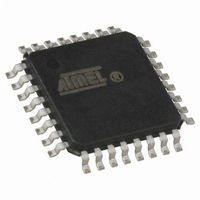
ATMEGA328P-AU Atmel, ATMEGA328P-AU Datasheet - Page 98

ATMEGA328P-AU
Manufacturer Part Number
ATMEGA328P-AU
Description
MCU AVR 32K FLASH 32TQFP
Manufacturer
Atmel
Series
AVR® ATmegar
Datasheets
1.ATMEGA48A-PU.pdf
(566 pages)
2.ATMEGA48A-PU.pdf
(33 pages)
3.ATMEGA48PA-MMH.pdf
(26 pages)
4.ATMEGA328P-AU.pdf
(567 pages)
Specifications of ATMEGA328P-AU
Core Processor
AVR
Core Size
8-Bit
Speed
20MHz
Connectivity
I²C, SPI, UART/USART
Peripherals
Brown-out Detect/Reset, POR, PWM, WDT
Number Of I /o
23
Program Memory Size
32KB (16K x 16)
Program Memory Type
FLASH
Eeprom Size
1K x 8
Ram Size
2K x 8
Voltage - Supply (vcc/vdd)
1.8 V ~ 5.5 V
Data Converters
A/D 8x10b
Oscillator Type
Internal
Operating Temperature
-40°C ~ 85°C
Package / Case
32-TQFP, 32-VQFP
Processor Series
ATMEGA32x
Core
AVR8
Data Bus Width
8 bit
Data Ram Size
2 KB
Interface Type
2-Wire, SPI, USART
Maximum Clock Frequency
20 MHz
Number Of Programmable I/os
23
Number Of Timers
3
Maximum Operating Temperature
+ 85 C
Mounting Style
SMD/SMT
3rd Party Development Tools
EWAVR, EWAVR-BL
Development Tools By Supplier
ATAVRDRAGON, ATSTK500, ATSTK600, ATAVRISP2, ATAVRONEKIT
Minimum Operating Temperature
- 40 C
On-chip Adc
10 bit, 8 Channel
Cpu Family
ATmega
Device Core
AVR
Device Core Size
8b
Frequency (max)
20MHz
Total Internal Ram Size
2KB
# I/os (max)
23
Number Of Timers - General Purpose
3
Operating Supply Voltage (typ)
2.5/3.3/5V
Operating Supply Voltage (max)
5.5V
Operating Supply Voltage (min)
1.8V
Instruction Set Architecture
RISC
Operating Temp Range
-40C to 85C
Operating Temperature Classification
Industrial
Mounting
Surface Mount
Pin Count
32
Package Type
TQFP
Controller Family/series
AVR MEGA
No. Of I/o's
23
Eeprom Memory Size
1KB
Ram Memory Size
2KB
Cpu Speed
20MHz
Rohs Compliant
Yes
For Use With
ATSTK600 - DEV KIT FOR AVR/AVR32770-1007 - ISP 4PORT ATMEL AVR MCU SPI/JTAGATAVRDRAGON - KIT DRAGON 32KB FLASH MEM AVR
Lead Free Status / RoHS Status
Lead free / RoHS Compliant
Other names
ATMEGA328P-20AU
ATMEGA328P-20AU
Q3790246
ATMEGA328P-20AU
Q3790246
Available stocks
Company
Part Number
Manufacturer
Quantity
Price
Company:
Part Number:
ATMEGA328P-AU
Manufacturer:
KINGBRIGHT
Quantity:
37 000
Company:
Part Number:
ATMEGA328P-AU
Manufacturer:
ATMEL
Quantity:
1 250
Part Number:
ATMEGA328P-AU
Manufacturer:
ATMEL/爱特梅尔
Quantity:
20 000
- ATMEGA48A-PU PDF datasheet
- ATMEGA48A-PU PDF datasheet #2
- ATMEGA48PA-MMH PDF datasheet #3
- ATMEGA328P-AU PDF datasheet #4
- Current page: 98 of 566
- Download datasheet (23Mb)
14.5
8271C–AVR–08/10
Output Compare Unit
The counting sequence is determined by the setting of the WGM01 and WGM00 bits located in
the Timer/Counter Control Register (TCCR0A) and the WGM02 bit located in the Timer/Counter
Control Register B (TCCR0B). There are close connections between how the counter behaves
(counts) and how waveforms are generated on the Output Compare outputs OC0A and OC0B.
For more details about advanced counting sequences and waveform generation, see
Operation” on page
The Timer/Counter Overflow Flag (TOV0) is set according to the mode of operation selected by
the WGM02:0 bits. TOV0 can be used for generating a CPU interrupt.
The 8-bit comparator continuously compares TCNT0 with the Output Compare Registers
(OCR0A and OCR0B). Whenever TCNT0 equals OCR0A or OCR0B, the comparator signals a
match. A match will set the Output Compare Flag (OCF0A or OCF0B) at the next timer clock
cycle. If the corresponding interrupt is enabled, the Output Compare Flag generates an Output
Compare interrupt. The Output Compare Flag is automatically cleared when the interrupt is exe-
cuted. Alternatively, the flag can be cleared by software by writing a logical one to its I/O bit
location. The Waveform Generator uses the match signal to generate an output according to
operating mode set by the WGM02:0 bits and Compare Output mode (COM0x1:0) bits. The max
and bottom signals are used by the Waveform Generator for handling the special cases of the
extreme values in some modes of operation
Figure 14-3
Figure 14-3. Output Compare Unit, Block Diagram
The OCR0x Registers are double buffered when using any of the Pulse Width Modulation
(PWM) modes. For the normal and Clear Timer on Compare (CTC) modes of operation, the dou-
ble buffering is disabled. The double buffering synchronizes the update of the OCR0x Compare
Registers to either top or bottom of the counting sequence. The synchronization prevents the
occurrence of odd-length, non-symmetrical PWM pulses, thereby making the output glitch-free.
ATmega48A/48PA/88A/88PA/168A/168PA/328/328
shows a block diagram of the Output Compare unit.
bottom
FOCn
top
100.
OCRnx
Waveform Generator
WGMn1:0
=
(8-bit Comparator )
DATA BUS
(”Modes of Operation” on page
COMnx1:0
TCNTn
OCFnx (Int.Req.)
OCnx
100).
”Modes of
98
Related parts for ATMEGA328P-AU
Image
Part Number
Description
Manufacturer
Datasheet
Request
R

Part Number:
Description:
Manufacturer:
Atmel Corporation
Datasheet:

Part Number:
Description:
Manufacturer:
ATMEL Corporation
Datasheet:

Part Number:
Description:
IC AVR MCU 32K 16MHZ 5V 44-QFN
Manufacturer:
Atmel
Datasheet:

Part Number:
Description:
IC AVR MCU 32K 16MHZ 5V 40DIP
Manufacturer:
Atmel
Datasheet:

Part Number:
Description:
IC AVR MCU 32K 16MHZ 5V 44TQFP
Manufacturer:
Atmel
Datasheet:

Part Number:
Description:
IC AVR MCU 32K 16MHZ IND 40-DIP
Manufacturer:
Atmel
Datasheet:

Part Number:
Description:
IC AVR MCU 32K 16MHZ IND 44-TQFP
Manufacturer:
Atmel
Datasheet:

Part Number:
Description:
MCU AVR 32KB FLASH 16MHZ 44TQFP
Manufacturer:
Atmel
Datasheet:

Part Number:
Description:
MCU AVR 32KB FLASH 16MHZ 44QFN
Manufacturer:
Atmel
Datasheet:

Part Number:
Description:
MCU AVR 32K FLASH 16MHZ 44-TQFP
Manufacturer:
Atmel
Datasheet:

Part Number:
Description:
IC AVR MCU 32K 16MHZ COM 40-DIP
Manufacturer:
Atmel
Datasheet:

Part Number:
Description:
IC AVR MCU 32K 16MHZ COM 44-QFN
Manufacturer:
Atmel
Datasheet:

Part Number:
Description:
IC AVR MCU 32K 16MHZ COM 44-TQFP
Manufacturer:
Atmel
Datasheet:


