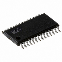
P89LPC932A1FDH,512 NXP Semiconductors, P89LPC932A1FDH,512 Datasheet - Page 22

P89LPC932A1FDH,512
Manufacturer Part Number
P89LPC932A1FDH,512
Description
IC 80C51 MCU FLASH 8K 28-TSSOP
Manufacturer
NXP Semiconductors
Series
LPC900r
Datasheet
1.P89LPC932A1FDH529.pdf
(64 pages)
Specifications of P89LPC932A1FDH,512
Program Memory Type
FLASH
Program Memory Size
8KB (8K x 8)
Package / Case
28-TSSOP
Core Processor
8051
Core Size
8-Bit
Speed
18MHz
Connectivity
I²C, SPI, UART/USART
Peripherals
Brown-out Detect/Reset, LED, POR, PWM, WDT
Number Of I /o
26
Ram Size
768 x 8
Voltage - Supply (vcc/vdd)
2.4 V ~ 3.6 V
Oscillator Type
Internal
Operating Temperature
-40°C ~ 85°C
Processor Series
P89LPC9x
Core
80C51
Data Bus Width
8 bit
Data Ram Size
768 B
Interface Type
I2C/SPI/UART
Maximum Clock Frequency
18 MHz
Number Of Programmable I/os
26
Number Of Timers
2
Operating Supply Voltage
2.4 V to 3.6 V
Maximum Operating Temperature
+ 85 C
Mounting Style
SMD/SMT
3rd Party Development Tools
PK51, CA51, A51, ULINK2
Minimum Operating Temperature
- 40 C
Cpu Family
89LP
Device Core
80C51
Device Core Size
8b
Frequency (max)
18MHz
Total Internal Ram Size
768Byte
# I/os (max)
26
Number Of Timers - General Purpose
2
Operating Supply Voltage (typ)
2.5/3.3V
Operating Supply Voltage (max)
3.6V
Operating Supply Voltage (min)
2.4V
Instruction Set Architecture
CISC
Operating Temp Range
-40C to 85C
Operating Temperature Classification
Industrial
Mounting
Surface Mount
Pin Count
28
Package Type
TSSOP
Lead Free Status / RoHS Status
Lead free / RoHS Compliant
For Use With
OM6292 - DEMO BOARD PCA2125 RTCDB-TSSOP-LPC932 - BOARD FOR LPC932 TSSOP622-1014 - BOARD FOR LPC9XX TSSOP622-1008 - BOARD FOR LPC9103 10-HVSON622-1006 - SOCKET ADAPTER BOARDMCB900K - BOARD PROTOTYPE NXP 89LPC9EPM900K - EMULATOR/PROGRAMMER NXP P89LPC9568-4000 - DEMO BOARD SPI/I2C TO DUAL UART568-3510 - DEMO BOARD SPI/I2C TO UART622-1003 - KIT FOR LCD DEMO622-1002 - USB IN-CIRCUIT PROG LPC9XX568-1759 - EMULATOR DEBUGGER/PROGRMMR LPC9X568-1758 - BOARD EVAL FOR LPC93X MCU FAMILY
Eeprom Size
-
Data Converters
-
Lead Free Status / Rohs Status
Lead free / RoHS Compliant
Other names
568-4515-5
935276132512
P89LPC932A1FDH
P89LPC932A1FDH
935276132512
P89LPC932A1FDH
P89LPC932A1FDH
NXP Semiconductors
Table 5.
[1]
P89LPC932A1_3
Product data sheet
Clock source
External clock input
Low/medium/high speed oscillator
(external crystal or resonator)
Required for operation above 12 MHz.
Number of I/O pins available
7.13.1.1 Quasi-bidirectional output configuration
7.13.1.2 Open-drain output configuration
7.13.1.3 Input-only configuration
7.13.1 Port configurations
All but three I/O port pins on the P89LPC932A1 may be configured by software to one of
four types on a bit-by-bit basis. These are: quasi-bidirectional (standard 80C51 port
outputs), push-pull, open drain, and input-only. Two configuration registers for each port
select the output type for each port pin.
Quasi-bidirectional output type can be used as both an input and output without the need
to reconfigure the port. This is possible because when the port outputs a logic HIGH, it is
weakly driven, allowing an external device to pull the pin LOW. When the pin is driven
LOW, it is driven strongly and able to sink a fairly large current. These features are
somewhat similar to an open-drain output except that there are three pull-up transistors in
the quasi-bidirectional output that serve different purposes.
The P89LPC932A1 is a 3 V device, but the pins are 5 V-tolerant. In quasi-bidirectional
mode, if a user applies 5 V on the pin, there will be a current flowing from the pin to V
causing extra power consumption. Therefore, applying 5 V in quasi-bidirectional mode is
discouraged.
A quasi-bidirectional port pin has a Schmitt trigger input that also has a glitch suppression
circuit.
The open-drain output configuration turns off all pull-ups and only drives the pull-down
transistor of the port driver when the port latch contains a logic 0. To be used as a logic
output, a port configured in this manner must have an external pull-up, typically a resistor
tied to V
An open-drain port pin has a Schmitt trigger input that also has a glitch suppression
circuit.
The input-only port configuration has no output drivers. It is a Schmitt trigger input that
also has a glitch suppression circuit.
1. P1.5 (RST) can only be an input and cannot be configured.
2. P1.2 (SCL/T0) and P1.3 (SDA/INT0) may only be configured to be either input-only or
open-drain.
DD
.
…continued
Reset option
No external reset (except during power-up)
External RST pin supported
No external reset (except during power-up)
External RST pin supported
Rev. 03 — 12 March 2007
8-bit microcontroller with accelerated two-clock 80C51 core
[1]
[1]
P89LPC932A1
Number of I/O pins
(28-pin package)
25
24
24
23
© NXP B.V. 2007. All rights reserved.
22 of 64
DD
,


