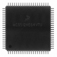
MC9S12NE64VTU Freescale Semiconductor, MC9S12NE64VTU Datasheet - Page 219

MC9S12NE64VTU
Manufacturer Part Number
MC9S12NE64VTU
Description
IC MCU 25MHZ ETHERNET/PHY 80TQFP
Manufacturer
Freescale Semiconductor
Series
HCS12r
Datasheet
1.MC9S12NE64VTU.pdf
(554 pages)
Specifications of MC9S12NE64VTU
Mfg Application Notes
MC9S12NE64 Integrated Ethernet Controller Implementing an Ethernet Interface with the MC9S12NE64 Web Server Development with MC9S12NE64 and Open TCP
Core Processor
HCS12
Core Size
16-Bit
Speed
25MHz
Connectivity
EBI/EMI, Ethernet, I²C, SCI, SPI
Peripherals
POR, PWM, WDT
Number Of I /o
38
Program Memory Size
64KB (64K x 8)
Program Memory Type
FLASH
Ram Size
8K x 8
Voltage - Supply (vcc/vdd)
2.375 V ~ 3.465 V
Data Converters
A/D 8x10b
Oscillator Type
Internal
Operating Temperature
-40°C ~ 105°C
Package / Case
80-TQFP Exposed Pad, 80-eTQFP, 80-HTQFP, 80-VQFP
Data Bus Width
16 bit
Data Ram Size
8 KB
Interface Type
I2C, SCI, SPI
Maximum Clock Frequency
25 MHz
Number Of Programmable I/os
70
Number Of Timers
16 bit
Operating Supply Voltage
- 0.3 V to + 3 V
Maximum Operating Temperature
+ 105 C
Mounting Style
SMD/SMT
Minimum Operating Temperature
- 65 C
On-chip Adc
10 bit
For Use With
EVB9S12NE64E - BOARD EVAL FOR 9S12NE64DEMO9S12NE64E - DEMO BOARD FOR 9S12NE64
Lead Free Status / RoHS Status
Lead free / RoHS Compliant
Eeprom Size
-
Lead Free Status / Rohs Status
Details
Available stocks
Company
Part Number
Manufacturer
Quantity
Price
Company:
Part Number:
MC9S12NE64VTU
Manufacturer:
FREESCALE
Quantity:
1 831
Company:
Part Number:
MC9S12NE64VTU
Manufacturer:
Freescale Semiconductor
Quantity:
10 000
Company:
Part Number:
MC9S12NE64VTUE
Manufacturer:
Freescale Semiconductor
Quantity:
10 000
Part Number:
MC9S12NE64VTUE
Manufacturer:
FREESCALE
Quantity:
20 000
- Current page: 219 of 554
- Download datasheet (4Mb)
7.3.2.6
This register selects the type of conversion sequence and the analog input channels sampled. Writes to this
register will abort current conversion sequence and start a new conversion sequence.
Read: Anytime
Write: Anytime
Freescale Semiconductor
CC, CB, CA
Reset
DSGN
SCAN
MULT
Field
DJM
2–0
7
6
5
4
W
R
DJM
Result Register Data Justification — This bit controls justification of conversion data in the result registers.
See
0 Left justified data in the result registers
1 Right justified data in the result registers
Result Register Data Signed or Unsigned Representation — This bit selects between signed and unsigned
conversion data representation in the result registers. Signed data is represented as 2’s complement. Signed
data is not available in right justification. See
for details.
0 Unsigned data representation in the result registers
1 Signed data representation in the result registers
Table 7-14
Table 7-15
signal range between 0 and 5.12 Volts.
Continuous Conversion Sequence Mode — This bit selects whether conversion sequences are performed
continuously or only once.
0 Single conversion sequence
1 Continuous conversion sequences (scan mode)
Multi-Channel Sample Mode — When MULT is 0, the ATD sequence controller samples only from the specified
analog input channel for an entire conversion sequence. The analog channel is selected by channel selection
code (control bits CC/CB/CA located in ATDCTL5). When MULT is 1, the ATD sequence controller samples
across channels. The number of channels sampled is determined by the sequence length value (S8C, S4C,
S2C, S1C). The first analog channel examined is determined by channel selection code (CC, CB, CA control
bits); subsequent channels sampled in the sequence are determined by incrementing the channel selection
code.
0 Sample only one channel
1 Sample across several channels
Analog Input Channel Select Code — These bits select the analog input channel(s) whose signals are
sampled and converted to digital codes.
channels. In the case of single channel scans (MULT = 0), this selection code specified the channel examined.
In the case of multi-channel scans (MULT = 1), this selection code represents the first channel to be examined
in the conversion sequence. Subsequent channels are determined by incrementing channel selection code;
selection codes that reach the maximum value wrap around to the minimum value.
ATD Control Register 5 (ATDCTL5)
0
7
Section 7.3.2.13, “ATD Conversion Result Registers (ATDDRx),”
= Unimplemented or Reserved
summarizes the result data formats available and how they are set up using the control bits.
illustrates the difference between the signed and unsigned, left justified output codes for an input
DSGN
0
6
Figure 7-8. ATD Control Register 5 (ATDCTL5)
Table 7-13. ATDCTL5 Field Descriptions
SCAN
MC9S12NE64 Data Sheet, Rev. 1.1
0
5
Table 7-16
MULT
0
4
Section 7.3.2.13, “ATD Conversion Result Registers (ATDDRx),”
Description
lists the coding used to select the various analog input
0
0
3
for details.
CC
0
2
Memory Map and Register Definition
CB
0
1
CA
0
0
219
Related parts for MC9S12NE64VTU
Image
Part Number
Description
Manufacturer
Datasheet
Request
R
Part Number:
Description:
Manufacturer:
Freescale Semiconductor, Inc
Datasheet:
Part Number:
Description:
Manufacturer:
Freescale Semiconductor, Inc
Datasheet:
Part Number:
Description:
Manufacturer:
Freescale Semiconductor, Inc
Datasheet:
Part Number:
Description:
Manufacturer:
Freescale Semiconductor, Inc
Datasheet:
Part Number:
Description:
Manufacturer:
Freescale Semiconductor, Inc
Datasheet:
Part Number:
Description:
Manufacturer:
Freescale Semiconductor, Inc
Datasheet:
Part Number:
Description:
Manufacturer:
Freescale Semiconductor, Inc
Datasheet:
Part Number:
Description:
Manufacturer:
Freescale Semiconductor, Inc
Datasheet:
Part Number:
Description:
Manufacturer:
Freescale Semiconductor, Inc
Datasheet:
Part Number:
Description:
Manufacturer:
Freescale Semiconductor, Inc
Datasheet:
Part Number:
Description:
Manufacturer:
Freescale Semiconductor, Inc
Datasheet:
Part Number:
Description:
Manufacturer:
Freescale Semiconductor, Inc
Datasheet:
Part Number:
Description:
Manufacturer:
Freescale Semiconductor, Inc
Datasheet:
Part Number:
Description:
Manufacturer:
Freescale Semiconductor, Inc
Datasheet:
Part Number:
Description:
Manufacturer:
Freescale Semiconductor, Inc
Datasheet:


