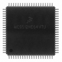
MC9S12NE64VTU Freescale Semiconductor, MC9S12NE64VTU Datasheet - Page 228

MC9S12NE64VTU
Manufacturer Part Number
MC9S12NE64VTU
Description
IC MCU 25MHZ ETHERNET/PHY 80TQFP
Manufacturer
Freescale Semiconductor
Series
HCS12r
Datasheet
1.MC9S12NE64VTU.pdf
(554 pages)
Specifications of MC9S12NE64VTU
Mfg Application Notes
MC9S12NE64 Integrated Ethernet Controller Implementing an Ethernet Interface with the MC9S12NE64 Web Server Development with MC9S12NE64 and Open TCP
Core Processor
HCS12
Core Size
16-Bit
Speed
25MHz
Connectivity
EBI/EMI, Ethernet, I²C, SCI, SPI
Peripherals
POR, PWM, WDT
Number Of I /o
38
Program Memory Size
64KB (64K x 8)
Program Memory Type
FLASH
Ram Size
8K x 8
Voltage - Supply (vcc/vdd)
2.375 V ~ 3.465 V
Data Converters
A/D 8x10b
Oscillator Type
Internal
Operating Temperature
-40°C ~ 105°C
Package / Case
80-TQFP Exposed Pad, 80-eTQFP, 80-HTQFP, 80-VQFP
Data Bus Width
16 bit
Data Ram Size
8 KB
Interface Type
I2C, SCI, SPI
Maximum Clock Frequency
25 MHz
Number Of Programmable I/os
70
Number Of Timers
16 bit
Operating Supply Voltage
- 0.3 V to + 3 V
Maximum Operating Temperature
+ 105 C
Mounting Style
SMD/SMT
Minimum Operating Temperature
- 65 C
On-chip Adc
10 bit
For Use With
EVB9S12NE64E - BOARD EVAL FOR 9S12NE64DEMO9S12NE64E - DEMO BOARD FOR 9S12NE64
Lead Free Status / RoHS Status
Lead free / RoHS Compliant
Eeprom Size
-
Lead Free Status / Rohs Status
Details
Available stocks
Company
Part Number
Manufacturer
Quantity
Price
Company:
Part Number:
MC9S12NE64VTU
Manufacturer:
FREESCALE
Quantity:
1 831
Company:
Part Number:
MC9S12NE64VTU
Manufacturer:
Freescale Semiconductor
Quantity:
10 000
Company:
Part Number:
MC9S12NE64VTUE
Manufacturer:
Freescale Semiconductor
Quantity:
10 000
Part Number:
MC9S12NE64VTUE
Manufacturer:
FREESCALE
Quantity:
20 000
- Current page: 228 of 554
- Download datasheet (4Mb)
Chapter 7 Analog-to-Digital Converter (ATD10B8CV3)
7.4.2.2
The input channel pins can be multiplexed between analog and digital data. As analog inputs, they are
multiplexed and sampled to supply signals to the A/D converter. As digital inputs, they supply external
input data that can be accessed through the digital port register PORTAD (input-only).
The analog/digital multiplex operation is performed in the input pads. The input pad is always connected
to the analog inputs of the ATD. The input pad signal is buffered to the digital port registers. This buffer
can be turned on or off with the ATDDIEN register. This is important so that the buffer does not draw
excess current when analog potentials are presented at its input.
7.4.2.3
The ATD can be configured for lower MCU power consumption in 3 different ways:
Note that the reset value for the ADPU bit is zero. Therefore, when this module is reset, it is reset into the
power down state.
7.5
At reset the ATD is in a power down state. The reset state of each individual bit is listed within the Register
Description section (see
and their bit-field.
7.6
The interrupt requested by the ATD is listed in
vector address and priority.
See register descriptions for further details.
228
1. Stop mode: This halts A/D conversion. Exit from stop mode will resume A/D conversion, but due
2. Wait mode with AWAI = 1: This halts A/D conversion. Exit from wait mode will resume A/D
3. Writing ADPU = 0 (Note that all ATD registers remain accessible.): This aborts any A/D
to the recovery time the result of this conversion should be ignored.
conversion, but due to the recovery time the result of this conversion should be ignored.
conversion in progress.
Resets
Interrupts
General Purpose Digital Input Port Operation
Low Power Modes
Section 7.3, “Memory Map and Register
Sequence complete
Interrupt Source
interrupt
Table 7-24. ATD Interrupt Vectors
MC9S12NE64 Data Sheet, Rev. 1.1
Table
Mask
CCR
I bit
7-24. Refer to the device overview chapter for related
ASCIE in ATDCTL2
Local Enable
Definition”), which details the registers
Freescale Semiconductor
Related parts for MC9S12NE64VTU
Image
Part Number
Description
Manufacturer
Datasheet
Request
R
Part Number:
Description:
Manufacturer:
Freescale Semiconductor, Inc
Datasheet:
Part Number:
Description:
Manufacturer:
Freescale Semiconductor, Inc
Datasheet:
Part Number:
Description:
Manufacturer:
Freescale Semiconductor, Inc
Datasheet:
Part Number:
Description:
Manufacturer:
Freescale Semiconductor, Inc
Datasheet:
Part Number:
Description:
Manufacturer:
Freescale Semiconductor, Inc
Datasheet:
Part Number:
Description:
Manufacturer:
Freescale Semiconductor, Inc
Datasheet:
Part Number:
Description:
Manufacturer:
Freescale Semiconductor, Inc
Datasheet:
Part Number:
Description:
Manufacturer:
Freescale Semiconductor, Inc
Datasheet:
Part Number:
Description:
Manufacturer:
Freescale Semiconductor, Inc
Datasheet:
Part Number:
Description:
Manufacturer:
Freescale Semiconductor, Inc
Datasheet:
Part Number:
Description:
Manufacturer:
Freescale Semiconductor, Inc
Datasheet:
Part Number:
Description:
Manufacturer:
Freescale Semiconductor, Inc
Datasheet:
Part Number:
Description:
Manufacturer:
Freescale Semiconductor, Inc
Datasheet:
Part Number:
Description:
Manufacturer:
Freescale Semiconductor, Inc
Datasheet:
Part Number:
Description:
Manufacturer:
Freescale Semiconductor, Inc
Datasheet:


