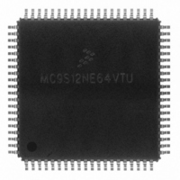
MC9S12NE64VTU Freescale Semiconductor, MC9S12NE64VTU Datasheet - Page 504

MC9S12NE64VTU
Manufacturer Part Number
MC9S12NE64VTU
Description
IC MCU 25MHZ ETHERNET/PHY 80TQFP
Manufacturer
Freescale Semiconductor
Series
HCS12r
Datasheet
1.MC9S12NE64VTU.pdf
(554 pages)
Specifications of MC9S12NE64VTU
Mfg Application Notes
MC9S12NE64 Integrated Ethernet Controller Implementing an Ethernet Interface with the MC9S12NE64 Web Server Development with MC9S12NE64 and Open TCP
Core Processor
HCS12
Core Size
16-Bit
Speed
25MHz
Connectivity
EBI/EMI, Ethernet, I²C, SCI, SPI
Peripherals
POR, PWM, WDT
Number Of I /o
38
Program Memory Size
64KB (64K x 8)
Program Memory Type
FLASH
Ram Size
8K x 8
Voltage - Supply (vcc/vdd)
2.375 V ~ 3.465 V
Data Converters
A/D 8x10b
Oscillator Type
Internal
Operating Temperature
-40°C ~ 105°C
Package / Case
80-TQFP Exposed Pad, 80-eTQFP, 80-HTQFP, 80-VQFP
Data Bus Width
16 bit
Data Ram Size
8 KB
Interface Type
I2C, SCI, SPI
Maximum Clock Frequency
25 MHz
Number Of Programmable I/os
70
Number Of Timers
16 bit
Operating Supply Voltage
- 0.3 V to + 3 V
Maximum Operating Temperature
+ 105 C
Mounting Style
SMD/SMT
Minimum Operating Temperature
- 65 C
On-chip Adc
10 bit
For Use With
EVB9S12NE64E - BOARD EVAL FOR 9S12NE64DEMO9S12NE64E - DEMO BOARD FOR 9S12NE64
Lead Free Status / RoHS Status
Lead free / RoHS Compliant
Eeprom Size
-
Lead Free Status / Rohs Status
Details
Available stocks
Company
Part Number
Manufacturer
Quantity
Price
Company:
Part Number:
MC9S12NE64VTU
Manufacturer:
FREESCALE
Quantity:
1 831
Company:
Part Number:
MC9S12NE64VTU
Manufacturer:
Freescale Semiconductor
Quantity:
10 000
Company:
Part Number:
MC9S12NE64VTUE
Manufacturer:
Freescale Semiconductor
Quantity:
10 000
Part Number:
MC9S12NE64VTUE
Manufacturer:
FREESCALE
Quantity:
20 000
- Current page: 504 of 554
- Download datasheet (4Mb)
Appendix A Electrical Characteristics
A.6
All ESD testing is in conformity with CDF-AEC-Q100 stress test qualification for automotive
grade integrated circuits. During the device qualification ESD stresses were performed for the
human body model (HBM), the machine model (MM), and the charge device model.
A device will be defined as a failure if after exposure to ESD pulses the device no longer meets the
device specification. Complete DC parametric and functional testing is performed per the
applicable device specification at room temperature followed by hot temperature, unless specified
otherwise in the device specification.
504
1
2
3
4
5
Num
The device contains an internal voltage regulator to generate the logic and PLL supply out of the I/O supply. The
absolute maximum ratings apply when the device is powered from an external source.
All digital I/O pins are internally clamped to V
These pins are internally clamped to V
This pin is clamped low to V
Maximum ambient temperature is package dependent.
10
11
12
13
14
15
1
2
3
4
5
6
7
8
9
ESD Protection and Latch-Up Immunity
I/O, Regulator and Analog Supply Voltage
Digital Logic Supply Voltage
PLL Supply Voltage
Voltage difference V
Voltage difference V
Digital I/O Input Voltage
Analog Reference
XFC, EXTAL, XTAL inputs
TEST input
Instantaneous Maximum Current
Single pin limit for all digital I/O pins
Instantaneous Maximum Current
Single pin limit for XFC, EXTAL, XTAL
Instantaneous Maximum Current
Single pin limit for TEST
Operating Temperature Range (ambient)
Operating Temperature Range (junction)
Storage Temperature Range
Table A-1. Absolute Maximum Ratings
DDX
SSX
1
SSPLL
Rating
to V
to V
4
, but not clamped high. This pin must be tied low in applications.
1
SSR
DDR
MC9S12NE64 Data Sheet, Rev. 1.1
SSPLL
and V
and V
2
and V
SSX
3
SSA
DDA
and V
DDPLL
DDX
.
, V
DDR
Symbol
V
V
∆
∆
V
RH,
V
DDPLL
V
V
VDDX
T
VSSX
V
TEST
I
or V
I
T
T
DD3
I
DL
DT
DD
ILV
stg
D
IN
A
J
V
RL
SSA
and V
–0.25
Min
–0.3
–0.3
–0.3
–0.3
–0.3
–0.3
–0.3
–0.3
–0.3
–25
–25
–40
–40
–65
DDA
.
Freescale Semiconductor
105
Max
10.0
+25
+25
140
155
4.5
3.0
3.0
0.3
0.3
6.5
6.5
3.0
0
5
Unit
mA
mA
mA
°C
°C
°C
V
V
V
V
V
V
V
V
V
Related parts for MC9S12NE64VTU
Image
Part Number
Description
Manufacturer
Datasheet
Request
R
Part Number:
Description:
Manufacturer:
Freescale Semiconductor, Inc
Datasheet:
Part Number:
Description:
Manufacturer:
Freescale Semiconductor, Inc
Datasheet:
Part Number:
Description:
Manufacturer:
Freescale Semiconductor, Inc
Datasheet:
Part Number:
Description:
Manufacturer:
Freescale Semiconductor, Inc
Datasheet:
Part Number:
Description:
Manufacturer:
Freescale Semiconductor, Inc
Datasheet:
Part Number:
Description:
Manufacturer:
Freescale Semiconductor, Inc
Datasheet:
Part Number:
Description:
Manufacturer:
Freescale Semiconductor, Inc
Datasheet:
Part Number:
Description:
Manufacturer:
Freescale Semiconductor, Inc
Datasheet:
Part Number:
Description:
Manufacturer:
Freescale Semiconductor, Inc
Datasheet:
Part Number:
Description:
Manufacturer:
Freescale Semiconductor, Inc
Datasheet:
Part Number:
Description:
Manufacturer:
Freescale Semiconductor, Inc
Datasheet:
Part Number:
Description:
Manufacturer:
Freescale Semiconductor, Inc
Datasheet:
Part Number:
Description:
Manufacturer:
Freescale Semiconductor, Inc
Datasheet:
Part Number:
Description:
Manufacturer:
Freescale Semiconductor, Inc
Datasheet:
Part Number:
Description:
Manufacturer:
Freescale Semiconductor, Inc
Datasheet:


