MC9S12NE64VTU Freescale Semiconductor, MC9S12NE64VTU Datasheet - Page 67
MC9S12NE64VTU
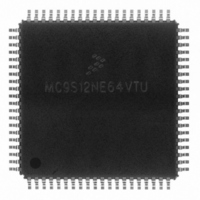
Manufacturer Part Number
MC9S12NE64VTU
Description
IC MCU 25MHZ ETHERNET/PHY 80TQFP
Manufacturer
Freescale Semiconductor
Series
HCS12r
Datasheet
1.MC9S12NE64VTU.pdf
(554 pages)
Specifications of MC9S12NE64VTU
Mfg Application Notes
MC9S12NE64 Integrated Ethernet Controller Implementing an Ethernet Interface with the MC9S12NE64 Web Server Development with MC9S12NE64 and Open TCP
Core Processor
HCS12
Core Size
16-Bit
Speed
25MHz
Connectivity
EBI/EMI, Ethernet, I²C, SCI, SPI
Peripherals
POR, PWM, WDT
Number Of I /o
38
Program Memory Size
64KB (64K x 8)
Program Memory Type
FLASH
Ram Size
8K x 8
Voltage - Supply (vcc/vdd)
2.375 V ~ 3.465 V
Data Converters
A/D 8x10b
Oscillator Type
Internal
Operating Temperature
-40°C ~ 105°C
Package / Case
80-TQFP Exposed Pad, 80-eTQFP, 80-HTQFP, 80-VQFP
Data Bus Width
16 bit
Data Ram Size
8 KB
Interface Type
I2C, SCI, SPI
Maximum Clock Frequency
25 MHz
Number Of Programmable I/os
70
Number Of Timers
16 bit
Operating Supply Voltage
- 0.3 V to + 3 V
Maximum Operating Temperature
+ 105 C
Mounting Style
SMD/SMT
Minimum Operating Temperature
- 65 C
On-chip Adc
10 bit
For Use With
EVB9S12NE64E - BOARD EVAL FOR 9S12NE64DEMO9S12NE64E - DEMO BOARD FOR 9S12NE64
Lead Free Status / RoHS Status
Lead free / RoHS Compliant
Eeprom Size
-
Lead Free Status / Rohs Status
Details
Available stocks
Company
Part Number
Manufacturer
Quantity
Price
Company:

Part Number:
MC9S12NE64VTU
Manufacturer:
FREESCALE
Quantity:
1 831
Company:
Part Number:
MC9S12NE64VTU
Manufacturer:
Freescale Semiconductor
Quantity:
10 000
Company:
Part Number:
MC9S12NE64VTUE
Manufacturer:
Freescale Semiconductor
Quantity:
10 000
Part Number:
MC9S12NE64VTUE
Manufacturer:
FREESCALE
Quantity:
20 000


Chapter 2
64 Kbyte Flash Module (S12FTS64KV3)
2.1
This document describes the FTS64K module that includes a 64Kbyte Flash (nonvolatile) memory. The
Flash memory may be read as either bytes, aligned words, or misaligned words. Read access time is one
bus cycle for bytes and aligned words, and two bus cycles for misaligned words.
The Flash memory is ideal for program and data storage for single-supply applications allowing for field
reprogramming without requiring external voltage sources for program or erase. Program and erase
functions are controlled by a command driven interface. The Flash module supports both block erase and
sector erase. An erased bit reads 1 and a programmed bit reads 0. The high voltage required to program
and erase the Flash memory is generated internally. It is not possible to read from a Flash block while it is
being erased or programmed.
2.1.1
Command Write Sequence — A three-step MCU instruction sequence to execute built-in algorithms
(including program and erase) on the Flash memory.
2.1.2
2.1.3
Program, erase, erase verify, and data compress operations (please refer to
Freescale Semiconductor
•
•
•
•
•
•
•
•
•
•
64 Kbytes of Flash memory comprised of one 64 Kbyte block divided into 128 sectors of 512 bytes
Automated program and erase algorithm
Interrupts on Flash command completion, command buffer empty
Fast sector erase and word program operation
2-stage command pipeline for faster multi-word program times
Sector erase abort feature for critical interrupt response
Flexible protection scheme to prevent accidental program or erase
Single power supply for all Flash operations including program and erase
Security feature to prevent unauthorized access to the Flash memory
Code integrity check using built-in data compression
Introduction
Glossary
Features
Modes of Operation
A Flash word must be in the erased state before being programmed.
Cumulative programming of bits within a Flash word is not allowed.
MC9S12NE64 Data Sheet, Rev. 1.1
CAUTION
Section 2.4.1
for details).
67
Related parts for MC9S12NE64VTU
Image
Part Number
Description
Manufacturer
Datasheet
Request
R

Part Number:
Description:
Manufacturer:
Freescale Semiconductor, Inc
Datasheet:
Part Number:
Description:
Manufacturer:
Freescale Semiconductor, Inc
Datasheet:
Part Number:
Description:
Manufacturer:
Freescale Semiconductor, Inc
Datasheet:
Part Number:
Description:
Manufacturer:
Freescale Semiconductor, Inc
Datasheet:
Part Number:
Description:
Manufacturer:
Freescale Semiconductor, Inc
Datasheet:
Part Number:
Description:
Manufacturer:
Freescale Semiconductor, Inc
Datasheet:
Part Number:
Description:
Manufacturer:
Freescale Semiconductor, Inc
Datasheet:
Part Number:
Description:
Manufacturer:
Freescale Semiconductor, Inc
Datasheet:
Part Number:
Description:
Manufacturer:
Freescale Semiconductor, Inc
Datasheet:
Part Number:
Description:
Manufacturer:
Freescale Semiconductor, Inc
Datasheet:
Part Number:
Description:
Manufacturer:
Freescale Semiconductor, Inc
Datasheet:
Part Number:
Description:
Manufacturer:
Freescale Semiconductor, Inc
Datasheet:
Part Number:
Description:
Manufacturer:
Freescale Semiconductor, Inc
Datasheet:
Part Number:
Description:
Manufacturer:
Freescale Semiconductor, Inc
Datasheet:
Part Number:
Description:
Manufacturer:
Freescale Semiconductor, Inc
Datasheet: