D13003TF16V Renesas Electronics America, D13003TF16V Datasheet - Page 317
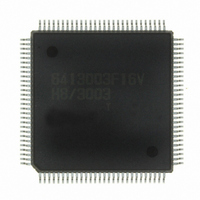
D13003TF16V
Manufacturer Part Number
D13003TF16V
Description
IC H8/3003 ROMLESS 112QFP
Manufacturer
Renesas Electronics America
Series
H8® H8/300Hr
Datasheet
1.D13003TF16V.pdf
(717 pages)
Specifications of D13003TF16V
Core Processor
H8/300H
Core Size
16-Bit
Speed
16MHz
Connectivity
SCI
Peripherals
DMA, PWM, WDT
Number Of I /o
50
Program Memory Type
ROMless
Ram Size
512 x 8
Voltage - Supply (vcc/vdd)
2.7 V ~ 5.5 V
Data Converters
A/D 8x10b
Oscillator Type
Internal
Operating Temperature
-20°C ~ 75°C
Package / Case
120-TQFP, 120-VQFP
Lead Free Status / RoHS Status
Lead free / RoHS Compliant
Eeprom Size
-
Program Memory Size
-
Available stocks
Company
Part Number
Manufacturer
Quantity
Price
Company:

Part Number:
D13003TF16V
Manufacturer:
RENESAS
Quantity:
210
Company:
Part Number:
D13003TF16V
Manufacturer:
Renesas Electronics America
Quantity:
10 000


When MDF is set to 1 to select phase counting mode, timer counter 2 (TCNT2) operates as an
up/down-counter and pins TCLKA and TCLKB become counter clock input pins. TCNT2 counts
both rising and falling edges of TCLKA and TCLKB, and counts up or down as follows.
Counting Direction
TCLKA pin
TCLKB pin
In phase counting mode channel 2 operates as above regardless of the external clock edges
selected by bits CKEG1 and CKEG0 and the clock source selected by bits TPSC2 to TPSC0 in
timer control register 2 (TCR2). Phase counting mode takes precedence over these settings.
The counter clearing condition selected by the CCLR1 and CCLR0 bits in TCR2 and the compare
match/input capture settings and interrupt functions of timer I/O control register 2 (TIOR2), timer
interrupt enable register 2 (TIER2), and timer status register 2 (TSR2) remain effective in phase
counting mode.
Bit 5—Flag Direction (FDIR): Designates the setting condition for the overflow flag (OVF) in
timer status register 2 (TSR2). The FDIR designation is valid in all modes in channel 2.
Bit 5
FDIR
0
1
Bit 4—PWM Mode 4 (PWM4): Selects whether channel 4 operates normally or in PWM mode.
Bit 4
PWM4
0
1
When bit PWM4 is set to 1 to select PWM mode, pin TIOCA4 becomes a PWM output pin. The
output goes to 1 at compare match with general register A4 (GRA4), and to 0 at compare match
with general register B4 (GRB4).
If complementary PWM mode or reset-synchronized PWM mode is selected by bits CMD1 and
CMD0 in the timer function control register (TFCR), the CMD1 and CMD0 setting takes
precedence and the PWM4 setting is ignored.
Description
OVF is set to 1 in TSR2 when TCNT2 overflows or underflows
OVF is set to 1 in TSR2 when TCNT2 overflows
Description
Channel 4 operates normally
Channel 4 operates in PWM mode
Down-Counting
Low
High
High
297
Low
Up-Counting
High
Low
Low
(Initial value)
(Initial value)
High
Related parts for D13003TF16V
Image
Part Number
Description
Manufacturer
Datasheet
Request
R

Part Number:
Description:
Rectifier diode. All purpose high power rectifier diodes, Non-controllable and half controlled rectifiers. Vrrm = 200V, Vrsm = 300V.
Manufacturer:
Usha Ltd.
Part Number:
Description:
Rectifier Diode, 800V, 130A, Silicon Diode, All purpose high power rectifier diode
Manufacturer:
Usha Ltd.

Part Number:
Description:
KIT STARTER FOR M16C/29
Manufacturer:
Renesas Electronics America
Datasheet:

Part Number:
Description:
KIT STARTER FOR R8C/2D
Manufacturer:
Renesas Electronics America
Datasheet:

Part Number:
Description:
R0K33062P STARTER KIT
Manufacturer:
Renesas Electronics America
Datasheet:

Part Number:
Description:
KIT STARTER FOR R8C/23 E8A
Manufacturer:
Renesas Electronics America
Datasheet:

Part Number:
Description:
KIT STARTER FOR R8C/25
Manufacturer:
Renesas Electronics America
Datasheet:

Part Number:
Description:
KIT STARTER H8S2456 SHARPE DSPLY
Manufacturer:
Renesas Electronics America
Datasheet:

Part Number:
Description:
KIT STARTER FOR R8C38C
Manufacturer:
Renesas Electronics America
Datasheet:

Part Number:
Description:
KIT STARTER FOR R8C35C
Manufacturer:
Renesas Electronics America
Datasheet:

Part Number:
Description:
KIT STARTER FOR R8CL3AC+LCD APPS
Manufacturer:
Renesas Electronics America
Datasheet:
Part Number:
Description:
KIT STARTER FOR RX610
Manufacturer:
Renesas Electronics America
Datasheet:

Part Number:
Description:
KIT STARTER FOR R32C/118
Manufacturer:
Renesas Electronics America
Datasheet:

Part Number:
Description:
KIT DEV RSK-R8C/26-29
Manufacturer:
Renesas Electronics America
Datasheet:

Part Number:
Description:
KIT STARTER FOR SH7124
Manufacturer:
Renesas Electronics America
Datasheet: