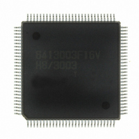
D13003TF16V Renesas Electronics America, D13003TF16V Datasheet - Page 418

D13003TF16V
Manufacturer Part Number
D13003TF16V
Description
IC H8/3003 ROMLESS 112QFP
Manufacturer
Renesas Electronics America
Series
H8® H8/300Hr
Datasheet
1.D13003TF16V.pdf
(717 pages)
Specifications of D13003TF16V
Core Processor
H8/300H
Core Size
16-Bit
Speed
16MHz
Connectivity
SCI
Peripherals
DMA, PWM, WDT
Number Of I /o
50
Program Memory Type
ROMless
Ram Size
512 x 8
Voltage - Supply (vcc/vdd)
2.7 V ~ 5.5 V
Data Converters
A/D 8x10b
Oscillator Type
Internal
Operating Temperature
-20°C ~ 75°C
Package / Case
120-TQFP, 120-VQFP
Lead Free Status / RoHS Status
Lead free / RoHS Compliant
Eeprom Size
-
Program Memory Size
-
Available stocks
Company
Part Number
Manufacturer
Quantity
Price
Company:
Part Number:
D13003TF16V
Manufacturer:
RENESAS
Quantity:
210
Company:
Part Number:
D13003TF16V
Manufacturer:
Renesas Electronics America
Quantity:
10 000
- Current page: 418 of 717
- Download datasheet (2Mb)
11.3 Operation
11.3.1 Overview
When corresponding bits in PADDR or PBDDR and NDERA or NDERB are set to 1, TPC output
is enabled. The TPC output initially consists of the corresponding PADR or PBDR contents.
When a compare-match event selected in TPCR occurs, the corresponding NDRA or NDRB bit
contents are transferred to PADR or PBDR to update the output values.
Figure 11-2 illustrates the TPC output operation. Table 11-3 summarizes the TPC operating
conditions.
Table 11-3 TPC Operating Conditions
NDER
0
1
Sequential output of up to 16-bit patterns is possible by writing new output data to NDRA and
NDRB before the next compare match. For information on non-overlapping operation, see
section 11.3.4, Non-Overlapping TPC Output.
TPC output pin
DDR
0
1
0
1
DDR
Q
Pin Function
Generic input port
Generic output port
Generic input port (but the DR bit is a read-only bit, and when compare
match occurs, the NDR bit value is transferred to the DR bit)
TPC pulse output
Figure 11-2 TPC Output Operation
Q
NDER
Q
DR
C
Output trigger signal
398
D
Q
NDR
D
Internal
data bus
Related parts for D13003TF16V
Image
Part Number
Description
Manufacturer
Datasheet
Request
R

Part Number:
Description:
Rectifier diode. All purpose high power rectifier diodes, Non-controllable and half controlled rectifiers. Vrrm = 200V, Vrsm = 300V.
Manufacturer:
Usha Ltd.

Part Number:
Description:
Rectifier Diode, 800V, 130A, Silicon Diode, All purpose high power rectifier diode
Manufacturer:
Usha Ltd.

Part Number:
Description:
KIT STARTER FOR M16C/29
Manufacturer:
Renesas Electronics America
Datasheet:

Part Number:
Description:
KIT STARTER FOR R8C/2D
Manufacturer:
Renesas Electronics America
Datasheet:

Part Number:
Description:
R0K33062P STARTER KIT
Manufacturer:
Renesas Electronics America
Datasheet:

Part Number:
Description:
KIT STARTER FOR R8C/23 E8A
Manufacturer:
Renesas Electronics America
Datasheet:

Part Number:
Description:
KIT STARTER FOR R8C/25
Manufacturer:
Renesas Electronics America
Datasheet:

Part Number:
Description:
KIT STARTER H8S2456 SHARPE DSPLY
Manufacturer:
Renesas Electronics America
Datasheet:

Part Number:
Description:
KIT STARTER FOR R8C38C
Manufacturer:
Renesas Electronics America
Datasheet:

Part Number:
Description:
KIT STARTER FOR R8C35C
Manufacturer:
Renesas Electronics America
Datasheet:

Part Number:
Description:
KIT STARTER FOR R8CL3AC+LCD APPS
Manufacturer:
Renesas Electronics America
Datasheet:

Part Number:
Description:
KIT STARTER FOR RX610
Manufacturer:
Renesas Electronics America
Datasheet:

Part Number:
Description:
KIT STARTER FOR R32C/118
Manufacturer:
Renesas Electronics America
Datasheet:

Part Number:
Description:
KIT DEV RSK-R8C/26-29
Manufacturer:
Renesas Electronics America
Datasheet:

Part Number:
Description:
KIT STARTER FOR SH7124
Manufacturer:
Renesas Electronics America
Datasheet:


