Z8F0413HH005EG Zilog, Z8F0413HH005EG Datasheet - Page 143
Z8F0413HH005EG
Manufacturer Part Number
Z8F0413HH005EG
Description
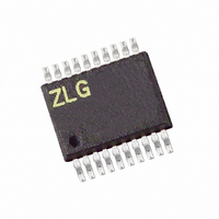
IC ENCORE MCU FLASH 4K 20SSOP
Manufacturer
Zilog
Series
Encore!® XP®r
Datasheet
1.Z8F0223SB005SG.pdf
(247 pages)
Specifications of Z8F0413HH005EG
Core Processor
Z8
Core Size
8-Bit
Speed
5MHz
Connectivity
IrDA, UART/USART
Peripherals
Brown-out Detect/Reset, LED, POR, PWM, WDT
Number Of I /o
16
Program Memory Size
4KB (4K x 8)
Program Memory Type
FLASH
Ram Size
1K x 8
Voltage - Supply (vcc/vdd)
2.7 V ~ 3.6 V
Oscillator Type
Internal
Operating Temperature
-40°C ~ 105°C
Package / Case
20-SSOP
For Use With
770-1002 - ISP 4PORT ZILOG Z8 ENCORE! MCU269-4643 - KIT DEV Z8 ENCORE XP 28-PIN269-4630 - DEV KIT FOR Z8 ENCORE 8K/4K269-4629 - KIT DEV Z8 ENCORE XP 28-PIN269-4628 - KIT DEV Z8 ENCORE XP 8-PIN
Lead Free Status / RoHS Status
Lead free / RoHS Compliant
Eeprom Size
-
Data Converters
-
Other names
269-4108
Z8F0413HH005EG
Z8F0413HH005EG


PS024314-0308
Caution:
Flash Operation Timing Using the Flash Frequency Registers
Flash Code Protection Against External Access
Flash Code Protection Against Accidental Program and Erasure
Before performing either a program or erase operation on Flash memory, you must first
configure the Flash Frequency High and Low Byte registers. The Flash Frequency regis-
ters allow programming and erasing of the Flash with system clock frequencies ranging
from 32 kHz (32768 Hz) through 20 MHz.
The Flash Frequency High and Low Byte registers combine to form a 16-bit value,
FFREQ, to control timing for Flash program and erase operations. The 16-bit binary Flash
Frequency value must contain the system clock frequency (in kHz). This value is
calculated using the following equation:
The user code contained within the Flash memory can be protected against external access
with the On-Chip Debugger. Programming the FRP Flash Option Bit prevents reading of
the user code with the On-Chip Debugger. For more information, see
page 141 and
Z8 Encore! XP F0823 Series provides several levels of protection against accidental pro-
gram and erasure of the Flash memory contents. This protection is provided by a combina-
tion of the Flash Option bits, the register locking mechanism, the page select redundancy
and the sector level protection control of the Flash Controller.
Flash Code Protection Using the Flash Option Bits
The FRP and FWP Flash Option Bits combine to provide three levels of Flash Program
Memory protection as listed in
page 141.
Flash programming and erasure are not supported for system clock frequencies below
32 kHz (32768 Hz) or above 20 MHz. The Flash Frequency High and Low Byte
registers must be loaded with the correct value to ensure operation of Z8 Encore! XP
F0823 Series devices.
FFREQ[15:0]
On-Chip Debugger
=
System Clock Frequency (Hz)
------------------------------------------------------------------------------ -
Table
on page 151.
1000
78. For more information, see
Z8 Encore! XP
Product Specification
Flash Option Bits
Flash Option Bits
®
F0823 Series
Flash Memory
on
on
®
133
Related parts for Z8F0413HH005EG
Image
Part Number
Description
Manufacturer
Datasheet
Request
R

Part Number:
Description:
Communication Controllers, ZILOG INTELLIGENT PERIPHERAL CONTROLLER (ZIP)
Manufacturer:
Zilog, Inc.
Datasheet:

Part Number:
Description:
KIT DEV FOR Z8 ENCORE 16K TO 64K
Manufacturer:
Zilog
Datasheet:

Part Number:
Description:
KIT DEV Z8 ENCORE XP 28-PIN
Manufacturer:
Zilog
Datasheet:

Part Number:
Description:
DEV KIT FOR Z8 ENCORE 8K/4K
Manufacturer:
Zilog
Datasheet:

Part Number:
Description:
KIT DEV Z8 ENCORE XP 28-PIN
Manufacturer:
Zilog
Datasheet:

Part Number:
Description:
DEV KIT FOR Z8 ENCORE 4K TO 8K
Manufacturer:
Zilog
Datasheet:
Part Number:
Description:
CMOS Z8 microcontroller. ROM 16 Kbytes, RAM 256 bytes, speed 16 MHz, 32 lines I/O, 3.0V to 5.5V
Manufacturer:
Zilog, Inc.
Datasheet:
Part Number:
Description:
Low-cost microcontroller. 512 bytes ROM, 61 bytes RAM, 8 MHz
Manufacturer:
Zilog, Inc.
Datasheet:
Part Number:
Description:
Z8 4K OTP Microcontroller
Manufacturer:
Zilog, Inc.
Datasheet:
Part Number:
Description:
CMOS SUPER8 ROMLESS MCU
Manufacturer:
Zilog, Inc.
Datasheet:
Part Number:
Description:
SL1866 CMOSZ8 OTP Microcontroller
Manufacturer:
Zilog, Inc.
Datasheet:
Part Number:
Description:
SL1866 CMOSZ8 OTP Microcontroller
Manufacturer:
Zilog, Inc.
Datasheet:
Part Number:
Description:
OTP (KB) = 1, RAM = 125, Speed = 12, I/O = 14, 8-bit Timers = 2, Comm Interfaces Other Features = Por, LV Protect, Voltage = 4.5-5.5V
Manufacturer:
Zilog, Inc.
Datasheet:
Part Number:
Description:
Manufacturer:
Zilog, Inc.
Datasheet: