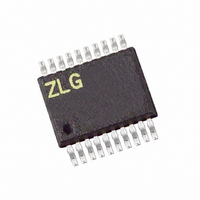
Z8F0413HH005EG Zilog, Z8F0413HH005EG Datasheet - Page 167

Z8F0413HH005EG
Manufacturer Part Number
Z8F0413HH005EG
Description
IC ENCORE MCU FLASH 4K 20SSOP
Manufacturer
Zilog
Series
Encore!® XP®r
Datasheet
1.Z8F0223SB005SG.pdf
(247 pages)
Specifications of Z8F0413HH005EG
Core Processor
Z8
Core Size
8-Bit
Speed
5MHz
Connectivity
IrDA, UART/USART
Peripherals
Brown-out Detect/Reset, LED, POR, PWM, WDT
Number Of I /o
16
Program Memory Size
4KB (4K x 8)
Program Memory Type
FLASH
Ram Size
1K x 8
Voltage - Supply (vcc/vdd)
2.7 V ~ 3.6 V
Oscillator Type
Internal
Operating Temperature
-40°C ~ 105°C
Package / Case
20-SSOP
For Use With
770-1002 - ISP 4PORT ZILOG Z8 ENCORE! MCU269-4643 - KIT DEV Z8 ENCORE XP 28-PIN269-4630 - DEV KIT FOR Z8 ENCORE 8K/4K269-4629 - KIT DEV Z8 ENCORE XP 28-PIN269-4628 - KIT DEV Z8 ENCORE XP 8-PIN
Lead Free Status / RoHS Status
Lead free / RoHS Compliant
Eeprom Size
-
Data Converters
-
Other names
269-4108
Z8F0413HH005EG
Z8F0413HH005EG
- Current page: 167 of 247
- Download datasheet (4Mb)
On-Chip Debugger Commands
PS024314-0308
Debug Command
Read OCD Revision
Reserved
Read OCD Status Register
Read Runtime Counter
Write OCD Control Register
Read OCD Control Register
Write Program Counter
Read Program Counter
Write Register
Read Register
Write Program Memory
Read Program Memory
Write Data Memory
Read Data Memory
Read Program Memory CRC
Reserved
Step Instruction
The host communicates to the OCD by sending OCD commands using the DBG interface.
During normal operation, only a subset of the OCD commands are available. In DEBUG
mode, all OCD commands become available unless the user code and control registers are
protected by programming the Flash Read Protect Option bit (
Protect Option bit prevents the code in memory from being read out of Z8 Encore! XP
F0823 Series products. When this option is enabled, several of the OCD commands are
disabled.
mand is described in further detail in the bulleted list following this table.
page 162 also indicates those commands that operate when the device is not in DEBUG
mode (normal operation) and those commands that are disabled by programming the Flash
Read Protect Option bit.
Table 99
Command
Byte
0CH
0DH
0AH
0BH
0EH
0FH
00H
01H
02H
03H
04H
05H
06H
07H
08H
09H
10H
on page 162 is a summary of the OCD commands. Each OCD com-
Enabled when
NOT in DEBUG
mode?
Yes
Yes
Yes
Yes
–
–
–
–
–
–
–
–
–
–
–
–
–
Disabled by Flash Read Protect
Option Bit
Only writes of the Flash Memory Control
the Mass Erase command is allowed to
registers are allowed. Additionally, only
be written to the Flash Control register.
Cannot clear DBGMODE bit.
Z8 Encore! XP
FRP
Product Specification
Disabled.
Disabled.
Disabled.
Disabled.
Disabled.
Disabled.
). The Flash Read
Yes.
–
–
–
–
–
–
–
–
®
On-Chip Debugger
Table 99
F0823 Series
on
®
157
Related parts for Z8F0413HH005EG
Image
Part Number
Description
Manufacturer
Datasheet
Request
R

Part Number:
Description:
Communication Controllers, ZILOG INTELLIGENT PERIPHERAL CONTROLLER (ZIP)
Manufacturer:
Zilog, Inc.
Datasheet:

Part Number:
Description:
KIT DEV FOR Z8 ENCORE 16K TO 64K
Manufacturer:
Zilog
Datasheet:

Part Number:
Description:
KIT DEV Z8 ENCORE XP 28-PIN
Manufacturer:
Zilog
Datasheet:

Part Number:
Description:
DEV KIT FOR Z8 ENCORE 8K/4K
Manufacturer:
Zilog
Datasheet:

Part Number:
Description:
KIT DEV Z8 ENCORE XP 28-PIN
Manufacturer:
Zilog
Datasheet:

Part Number:
Description:
DEV KIT FOR Z8 ENCORE 4K TO 8K
Manufacturer:
Zilog
Datasheet:

Part Number:
Description:
CMOS Z8 microcontroller. ROM 16 Kbytes, RAM 256 bytes, speed 16 MHz, 32 lines I/O, 3.0V to 5.5V
Manufacturer:
Zilog, Inc.
Datasheet:

Part Number:
Description:
Low-cost microcontroller. 512 bytes ROM, 61 bytes RAM, 8 MHz
Manufacturer:
Zilog, Inc.
Datasheet:

Part Number:
Description:
Z8 4K OTP Microcontroller
Manufacturer:
Zilog, Inc.
Datasheet:

Part Number:
Description:
CMOS SUPER8 ROMLESS MCU
Manufacturer:
Zilog, Inc.
Datasheet:

Part Number:
Description:
SL1866 CMOSZ8 OTP Microcontroller
Manufacturer:
Zilog, Inc.
Datasheet:

Part Number:
Description:
SL1866 CMOSZ8 OTP Microcontroller
Manufacturer:
Zilog, Inc.
Datasheet:

Part Number:
Description:
OTP (KB) = 1, RAM = 125, Speed = 12, I/O = 14, 8-bit Timers = 2, Comm Interfaces Other Features = Por, LV Protect, Voltage = 4.5-5.5V
Manufacturer:
Zilog, Inc.
Datasheet:

Part Number:
Description:
Manufacturer:
Zilog, Inc.
Datasheet:


