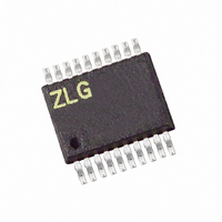
Z8F0413HH005EG Zilog, Z8F0413HH005EG Datasheet - Page 83

Z8F0413HH005EG
Manufacturer Part Number
Z8F0413HH005EG
Description
IC ENCORE MCU FLASH 4K 20SSOP
Manufacturer
Zilog
Series
Encore!® XP®r
Datasheet
1.Z8F0223SB005SG.pdf
(247 pages)
Specifications of Z8F0413HH005EG
Core Processor
Z8
Core Size
8-Bit
Speed
5MHz
Connectivity
IrDA, UART/USART
Peripherals
Brown-out Detect/Reset, LED, POR, PWM, WDT
Number Of I /o
16
Program Memory Size
4KB (4K x 8)
Program Memory Type
FLASH
Ram Size
1K x 8
Voltage - Supply (vcc/vdd)
2.7 V ~ 3.6 V
Oscillator Type
Internal
Operating Temperature
-40°C ~ 105°C
Package / Case
20-SSOP
For Use With
770-1002 - ISP 4PORT ZILOG Z8 ENCORE! MCU269-4643 - KIT DEV Z8 ENCORE XP 28-PIN269-4630 - DEV KIT FOR Z8 ENCORE 8K/4K269-4629 - KIT DEV Z8 ENCORE XP 28-PIN269-4628 - KIT DEV Z8 ENCORE XP 8-PIN
Lead Free Status / RoHS Status
Lead free / RoHS Compliant
Eeprom Size
-
Data Converters
-
Other names
269-4108
Z8F0413HH005EG
Z8F0413HH005EG
- Current page: 83 of 247
- Download datasheet (4Mb)
PS024314-0308
If an initial starting value other than
registers, use the ONE-SHOT mode equation to determine the first PWM time-out period.
If TPOL is set to 0, the ratio of the PWM output High time to the total period is
represented by the following equation:
If TPOL is set to 1, the ratio of the PWM output High time to the total period is
represented by the following equation:
PWM Dual Output Mode
In PWM DUAL OUTPUT mode, the timer outputs a PWM output signal pair (basic PWM
signal and its complement) through two GPIO port pins. The timer input is the system
clock. The timer first counts up to the 16-bit PWM match value stored in the Timer PWM
High and Low Byte registers. When the timer count value matches the PWM value, the
Timer Output toggles. The timer continues counting until it reaches the Reload value
stored in the Timer Reload High and Low Byte registers. Upon reaching the Reload value,
the timer generates an interrupt, the count value in the Timer High and Low Byte registers
is reset to
If the TPOL bit in the Timer Control register is set to 1, the Timer Output signal begins as
a High (1) and transitions to a Low (0) when the timer value matches the PWM value. The
Timer Output signal returns to a High (1) after the timer reaches the Reload value and is
reset to
If the TPOL bit in the Timer Control register is set to 0, the Timer Output signal begins as
a Low (0) and transitions to a High (1) when the timer value matches the PWM value. The
Timer Output signal returns to a Low (0) after the timer reaches the Reload value and is
reset to
The timer also generates a second PWM output signal Timer Output Complement. The
Timer Output Complement is the complement of the Timer Output PWM signal. A
programmable deadband delay can be configured to time delay (0 to 128 system clock
cycles) PWM output transitions on these two pins from a low to a high (inactive to active).
This ensures a time gap between the deassertion of one PWM output to the assertion of its
complement.
Follow the steps below for configuring a timer for PWM Dual Output mode and initiating
the PWM operation:
1. Write to the Timer Control register to:
–
–
–
PWM Output High Time Ratio (%)
PWM Output High Time Ratio (%)
0001H
0001H
Disable the timer
Configure the timer for PWM Dual Output mode. Setting the mode also involves
writing to TMODEHI bit in TxCTL1 register
Set the prescale value
0001H
.
.
and counting resumes.
0001H
=
=
is loaded into the Timer High and Low Byte
----------------------------------- - 100
Reload Value
Reload Value
------------------------------------------------------------------ -
PWM Value
Reload Value
Z8 Encore! XP
×
–
PWM Value
Product Specification
®
×
F0823 Series
100
Timers
73
Related parts for Z8F0413HH005EG
Image
Part Number
Description
Manufacturer
Datasheet
Request
R

Part Number:
Description:
Communication Controllers, ZILOG INTELLIGENT PERIPHERAL CONTROLLER (ZIP)
Manufacturer:
Zilog, Inc.
Datasheet:

Part Number:
Description:
KIT DEV FOR Z8 ENCORE 16K TO 64K
Manufacturer:
Zilog
Datasheet:

Part Number:
Description:
KIT DEV Z8 ENCORE XP 28-PIN
Manufacturer:
Zilog
Datasheet:

Part Number:
Description:
DEV KIT FOR Z8 ENCORE 8K/4K
Manufacturer:
Zilog
Datasheet:

Part Number:
Description:
KIT DEV Z8 ENCORE XP 28-PIN
Manufacturer:
Zilog
Datasheet:

Part Number:
Description:
DEV KIT FOR Z8 ENCORE 4K TO 8K
Manufacturer:
Zilog
Datasheet:

Part Number:
Description:
CMOS Z8 microcontroller. ROM 16 Kbytes, RAM 256 bytes, speed 16 MHz, 32 lines I/O, 3.0V to 5.5V
Manufacturer:
Zilog, Inc.
Datasheet:

Part Number:
Description:
Low-cost microcontroller. 512 bytes ROM, 61 bytes RAM, 8 MHz
Manufacturer:
Zilog, Inc.
Datasheet:

Part Number:
Description:
Z8 4K OTP Microcontroller
Manufacturer:
Zilog, Inc.
Datasheet:

Part Number:
Description:
CMOS SUPER8 ROMLESS MCU
Manufacturer:
Zilog, Inc.
Datasheet:

Part Number:
Description:
SL1866 CMOSZ8 OTP Microcontroller
Manufacturer:
Zilog, Inc.
Datasheet:

Part Number:
Description:
SL1866 CMOSZ8 OTP Microcontroller
Manufacturer:
Zilog, Inc.
Datasheet:

Part Number:
Description:
OTP (KB) = 1, RAM = 125, Speed = 12, I/O = 14, 8-bit Timers = 2, Comm Interfaces Other Features = Por, LV Protect, Voltage = 4.5-5.5V
Manufacturer:
Zilog, Inc.
Datasheet:

Part Number:
Description:
Manufacturer:
Zilog, Inc.
Datasheet:


