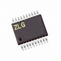
Z8F0413HH005EG Zilog, Z8F0413HH005EG Datasheet - Page 46

Z8F0413HH005EG
Manufacturer Part Number
Z8F0413HH005EG
Description
IC ENCORE MCU FLASH 4K 20SSOP
Manufacturer
Zilog
Series
Encore!® XP®r
Datasheet
1.Z8F0223SB005SG.pdf
(247 pages)
Specifications of Z8F0413HH005EG
Core Processor
Z8
Core Size
8-Bit
Speed
5MHz
Connectivity
IrDA, UART/USART
Peripherals
Brown-out Detect/Reset, LED, POR, PWM, WDT
Number Of I /o
16
Program Memory Size
4KB (4K x 8)
Program Memory Type
FLASH
Ram Size
1K x 8
Voltage - Supply (vcc/vdd)
2.7 V ~ 3.6 V
Oscillator Type
Internal
Operating Temperature
-40°C ~ 105°C
Package / Case
20-SSOP
For Use With
770-1002 - ISP 4PORT ZILOG Z8 ENCORE! MCU269-4643 - KIT DEV Z8 ENCORE XP 28-PIN269-4630 - DEV KIT FOR Z8 ENCORE 8K/4K269-4629 - KIT DEV Z8 ENCORE XP 28-PIN269-4628 - KIT DEV Z8 ENCORE XP 8-PIN
Lead Free Status / RoHS Status
Lead free / RoHS Compliant
Eeprom Size
-
Data Converters
-
Other names
269-4108
Z8F0413HH005EG
Z8F0413HH005EG
- Current page: 46 of 247
- Download datasheet (4Mb)
Architecture
GPIO Alternate Functions
PS024314-0308
System
DATA
Clock
Bus
Data Register
Port Output
Figure 7
the ability to accommodate alternate functions and variable port current drive strength is
not displayed.
Many of the GPIO port pins are used for general-purpose I/O and access to on-chip
peripheral functions such as the timers and serial communication devices. The port A–D
Alternate Function sub-registers configure these pins for either GPIO or alternate function
operation. When a pin is configured for alternate function, control of the port pin direction
(input/output) is passed from the Port A–D Data Direction registers to the alternate func-
tion assigned to this pin.
each port pin. The alternate function associated at a pin is defined through Alternate
Function Sets sub-registers AFS1 and AFS2.
The crystal oscillator functionality is not controlled by the GPIO block. When the crystal
oscillator is enabled in the oscillator control block, the GPIO functionality of PA0 and PA1
is overridden. In that case, those pins function as input and output for the crystal oscillator.
D
Q
displays a simplified block diagram of a GPIO port pin. In this figure,
Figure 7. GPIO Port Pin Block Diagram
System
Clock
Port Output Control
Port Data Direction
Table 15
Data Register
Port Input
Q
on page 39 lists the alternate functions possible with
D
Q
Z8 Encore! XP
D
General-Purpose Input/Output
Schmitt-Trigger
Product Specification
GND
VDD
®
F0823 Series
Port
Pin
36
Related parts for Z8F0413HH005EG
Image
Part Number
Description
Manufacturer
Datasheet
Request
R

Part Number:
Description:
Communication Controllers, ZILOG INTELLIGENT PERIPHERAL CONTROLLER (ZIP)
Manufacturer:
Zilog, Inc.
Datasheet:

Part Number:
Description:
KIT DEV FOR Z8 ENCORE 16K TO 64K
Manufacturer:
Zilog
Datasheet:

Part Number:
Description:
KIT DEV Z8 ENCORE XP 28-PIN
Manufacturer:
Zilog
Datasheet:

Part Number:
Description:
DEV KIT FOR Z8 ENCORE 8K/4K
Manufacturer:
Zilog
Datasheet:

Part Number:
Description:
KIT DEV Z8 ENCORE XP 28-PIN
Manufacturer:
Zilog
Datasheet:

Part Number:
Description:
DEV KIT FOR Z8 ENCORE 4K TO 8K
Manufacturer:
Zilog
Datasheet:

Part Number:
Description:
CMOS Z8 microcontroller. ROM 16 Kbytes, RAM 256 bytes, speed 16 MHz, 32 lines I/O, 3.0V to 5.5V
Manufacturer:
Zilog, Inc.
Datasheet:

Part Number:
Description:
Low-cost microcontroller. 512 bytes ROM, 61 bytes RAM, 8 MHz
Manufacturer:
Zilog, Inc.
Datasheet:

Part Number:
Description:
Z8 4K OTP Microcontroller
Manufacturer:
Zilog, Inc.
Datasheet:

Part Number:
Description:
CMOS SUPER8 ROMLESS MCU
Manufacturer:
Zilog, Inc.
Datasheet:

Part Number:
Description:
SL1866 CMOSZ8 OTP Microcontroller
Manufacturer:
Zilog, Inc.
Datasheet:

Part Number:
Description:
SL1866 CMOSZ8 OTP Microcontroller
Manufacturer:
Zilog, Inc.
Datasheet:

Part Number:
Description:
OTP (KB) = 1, RAM = 125, Speed = 12, I/O = 14, 8-bit Timers = 2, Comm Interfaces Other Features = Por, LV Protect, Voltage = 4.5-5.5V
Manufacturer:
Zilog, Inc.
Datasheet:

Part Number:
Description:
Manufacturer:
Zilog, Inc.
Datasheet:


