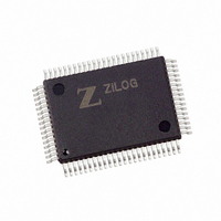
Z16F2811FI20SG Zilog, Z16F2811FI20SG Datasheet - Page 134

Z16F2811FI20SG
Manufacturer Part Number
Z16F2811FI20SG
Description
IC ZNEO MCU FLASH 128K 80QFP
Manufacturer
Zilog
Series
Encore!® ZNEOr
Specifications of Z16F2811FI20SG
Core Processor
ZNEO
Core Size
16-Bit
Speed
20MHz
Connectivity
EBI/EMI, I²C, IrDA, LIN, SPI, UART/USART
Peripherals
Brown-out Detect/Reset, DMA, POR, PWM, WDT
Number Of I /o
60
Program Memory Size
128KB (128K x 8)
Program Memory Type
FLASH
Ram Size
4K x 8
Voltage - Supply (vcc/vdd)
2.7 V ~ 3.6 V
Data Converters
A/D 12x10b
Oscillator Type
Internal
Operating Temperature
0°C ~ 70°C
Package / Case
80-BQFP
Processor Series
Z16F2x
Core
Zneo
Data Bus Width
16 bit
Data Ram Size
4 B
Interface Type
ESPI, I2C, UART
Maximum Clock Frequency
20 MHz
Number Of Programmable I/os
60
Number Of Timers
4
Operating Supply Voltage
2.7 V to 3.6 V
Maximum Operating Temperature
+ 70 C
Mounting Style
SMD/SMT
Development Tools By Supplier
Z16F2800100ZCOG
Minimum Operating Temperature
0 C
On-chip Adc
10 bit, 12 Channel
For Use With
770-1003 - ISP 4PORT FOR ZILOG ZNEO MCU269-4537 - DEV KIT FOR Z16F ZNEO
Lead Free Status / RoHS Status
Lead free / RoHS Compliant
Eeprom Size
-
Lead Free Status / Rohs Status
Details
Other names
269-4534
Available stocks
Company
Part Number
Manufacturer
Quantity
Price
Company:
Part Number:
Z16F2811FI20SG
Manufacturer:
Zilog
Quantity:
155
- Current page: 134 of 388
- Download datasheet (22Mb)
PS022008-0810
Manual Off-state Control of PWM Output Channels
Deadband Insertion
Minimum PWM Pulse Width Filter
and transits to the off-state when the PWM timer count reaches the programmed duty
cycle. The low-side PWM value starts in the off-state and transits to the on-state as the
PWM timer count reaches the value in the associated duty cycle register. Alternately,
setting the POLx causes the high-side output to start in the off-state and the low-side
output to start in the on-state.
Each PWM output is controlled directly by the modulator logic or set to the off-state. To
manually set the PWM output to the off-state, set the OUTCTL bit and the associated
OUTx
individually by channel. For example, suppressing a single output of pair allows the
complementary channel to continue operating. Similarly, if the outputs are operating
independently disabling one output channel has no effect on the other PWM outputs.
When the PWM outputs are configured to operate as complementary pairs, an 8-bit
deadband value is defined in the
time causes the modulator to separate the deassertion of one PWM signal from the
assertion of its complement. This is essential for many motor control applications to
prevent simultaneous turn-on of the high-side and low-side drive transistors. The
deadband counter directly counts system clock cycles and is unaffected by PWM prescaler
settings. The width of this deadband is the number of system clock cycles specified in the
PWM Deadband Register
clocks and the maximum time is 255 system clocks. Both PWM outputs of a
complementary pair is deasserted during the deadband period. Generation of deadband
time does not alter the PWM period but the deadband time is subtracted from the active
time of the PWM outputs.
on the PWM output.
The PWM modulator is capable of producing pulses as narrow as a single system clock
cycle in width. The response time of external drive circuit is slower than the period of a
system clock. Therefore, a filter is implemented to enforce a minimum width pulse on the
PWM output pins. All output pulses, either High or Low, must be at least the minimum
number of PWM clock cycles (for more details, see
as specified in the
expected pulse width is less than the threshold, the associated PWM output does not
change state until the duty cycle value has changed sufficiently to allow pulse generation
of an acceptable width. The minimum pulse width filter also accounts for the duty cycle
variation caused by the deadband insertion. The PWM output pulse is filtered even if the
bits in the
PWM Output Control Register
PWM Minimum Pulse Width Filter (PWMMPF)
(PWMDB). The minimum deadband duration is zero system
Figure 21
P R E L I M I N A R Y
PWM Deadband Register
on page 117 displays the effect of deadband insertion
(PWMOUT). Off-state control operates
PWM Prescaler
(PWMDB). Inserting deadband
Multi-Channel PWM Timer
Product Specification
ZNEO
on page 116) in width
register. If the
Z16F Series
119
Related parts for Z16F2811FI20SG
Image
Part Number
Description
Manufacturer
Datasheet
Request
R

Part Number:
Description:
High Performance Microcontrollers
Manufacturer:
ZiLOG Semiconductor
Datasheet:

Part Number:
Description:
Communication Controllers, ZILOG INTELLIGENT PERIPHERAL CONTROLLER (ZIP)
Manufacturer:
Zilog, Inc.
Datasheet:

Part Number:
Description:
KIT DEV FOR Z8 ENCORE 16K TO 64K
Manufacturer:
Zilog
Datasheet:

Part Number:
Description:
KIT DEV Z8 ENCORE XP 28-PIN
Manufacturer:
Zilog
Datasheet:

Part Number:
Description:
DEV KIT FOR Z8 ENCORE 8K/4K
Manufacturer:
Zilog
Datasheet:

Part Number:
Description:
KIT DEV Z8 ENCORE XP 28-PIN
Manufacturer:
Zilog
Datasheet:

Part Number:
Description:
DEV KIT FOR Z8 ENCORE 4K TO 8K
Manufacturer:
Zilog
Datasheet:

Part Number:
Description:
CMOS Z8 microcontroller. ROM 16 Kbytes, RAM 256 bytes, speed 16 MHz, 32 lines I/O, 3.0V to 5.5V
Manufacturer:
Zilog, Inc.
Datasheet:

Part Number:
Description:
Low-cost microcontroller. 512 bytes ROM, 61 bytes RAM, 8 MHz
Manufacturer:
Zilog, Inc.
Datasheet:

Part Number:
Description:
Z8 4K OTP Microcontroller
Manufacturer:
Zilog, Inc.
Datasheet:

Part Number:
Description:
CMOS SUPER8 ROMLESS MCU
Manufacturer:
Zilog, Inc.
Datasheet:

Part Number:
Description:
SL1866 CMOSZ8 OTP Microcontroller
Manufacturer:
Zilog, Inc.
Datasheet:

Part Number:
Description:
SL1866 CMOSZ8 OTP Microcontroller
Manufacturer:
Zilog, Inc.
Datasheet:

Part Number:
Description:
OTP (KB) = 1, RAM = 125, Speed = 12, I/O = 14, 8-bit Timers = 2, Comm Interfaces Other Features = Por, LV Protect, Voltage = 4.5-5.5V
Manufacturer:
Zilog, Inc.
Datasheet:


