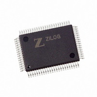
Z16F2811FI20SG Zilog, Z16F2811FI20SG Datasheet - Page 230

Z16F2811FI20SG
Manufacturer Part Number
Z16F2811FI20SG
Description
IC ZNEO MCU FLASH 128K 80QFP
Manufacturer
Zilog
Series
Encore!® ZNEOr
Specifications of Z16F2811FI20SG
Core Processor
ZNEO
Core Size
16-Bit
Speed
20MHz
Connectivity
EBI/EMI, I²C, IrDA, LIN, SPI, UART/USART
Peripherals
Brown-out Detect/Reset, DMA, POR, PWM, WDT
Number Of I /o
60
Program Memory Size
128KB (128K x 8)
Program Memory Type
FLASH
Ram Size
4K x 8
Voltage - Supply (vcc/vdd)
2.7 V ~ 3.6 V
Data Converters
A/D 12x10b
Oscillator Type
Internal
Operating Temperature
0°C ~ 70°C
Package / Case
80-BQFP
Processor Series
Z16F2x
Core
Zneo
Data Bus Width
16 bit
Data Ram Size
4 B
Interface Type
ESPI, I2C, UART
Maximum Clock Frequency
20 MHz
Number Of Programmable I/os
60
Number Of Timers
4
Operating Supply Voltage
2.7 V to 3.6 V
Maximum Operating Temperature
+ 70 C
Mounting Style
SMD/SMT
Development Tools By Supplier
Z16F2800100ZCOG
Minimum Operating Temperature
0 C
On-chip Adc
10 bit, 12 Channel
For Use With
770-1003 - ISP 4PORT FOR ZILOG ZNEO MCU269-4537 - DEV KIT FOR Z16F ZNEO
Lead Free Status / RoHS Status
Lead free / RoHS Compliant
Eeprom Size
-
Lead Free Status / Rohs Status
Details
Other names
269-4534
Available stocks
Company
Part Number
Manufacturer
Quantity
Price
Company:
Part Number:
Z16F2811FI20SG
Manufacturer:
Zilog
Quantity:
155
- Current page: 230 of 388
- Download datasheet (22Mb)
PS022008-0810
S
Figure 45. Data Transfer Format - Master Read Transaction with 7-Bit Address
or the START bit (end this transaction, start a new one). The transmit data register is
flushed automatically.
Master Read Transaction with a 7-Bit Address
Figure 45
The procedure for a Master read operation to a 7-bit addressed Slave is as follows:
1. Software initializes the MODE field in the I
2. Software writes the I
3. Software asserts the START bit of the I
4. If this is a single byte transfer, software asserts the NAK bit of the I
5. The I
6. The I
7. The I
8. The I
9. The I
10. Software responds by reading the I
11. The I
Address
with 7- or 10-bit addressing (I
The MODE field selects the address width for this node when addressed as a Slave,
not for the remote Slave. Software asserts the IEN bit in the I
so that after the first byte of data has been read by the I
Acknowledge instruction is sent to the I
next High period of SCL.
If the slave does not acknowledge the address byte, the I
bit in the I
register. Software responds to the Not Acknowledge interrupt by setting the STOP bit
and clearing the TXI bit. The I
the STOP condition on the bus and clears the STOP and NCKI bits. The transaction is
complete (ignore the following steps).
signal.
last, software must set the
else an Acknowledge.
Slave
2
2
2
2
2
2
displays the data transfer format for a read operation to a 7-bit addressed Slave.
C Controller sends the START condition.
C Controller sends the address and read bit out the SDA signal.
C Slave acknowledges the address by pulling the SDA signal Low during the
C Controller shifts in the first byte of data from the I
C Controller asserts the Receive interrupt.
C Controller sends a Not Acknowledge to the I
2
C Status register, sets the
R=1
2
C Data register with a 7-bit Slave address plus the read bit (=1).
P R E L I M I N A R Y
NAK
A
2
2
C bus protocol allows mixing Slave address types).
bit of the I
C Controller flushes the transmit data register, sends
2
C Data register. If the next data byte is to be the
ACKV
Data
2
2
C Control register.
C Slave.
2
C Control register.
bit and clears the
2
C Mode register for Master/Slave mode
A
2
C Slave if this is the last byte,
2
C Controller, a Not
2
C Controller sets the NCKI
I
2
2
C Master/Slave Controller
C Slave on the SDA
Product Specification
Data
ACK
2
C Control register.
ZNEO
bit in the I
2
C Control register
Z16F Series
A
2
C State
P/S
214
Related parts for Z16F2811FI20SG
Image
Part Number
Description
Manufacturer
Datasheet
Request
R

Part Number:
Description:
High Performance Microcontrollers
Manufacturer:
ZiLOG Semiconductor
Datasheet:

Part Number:
Description:
Communication Controllers, ZILOG INTELLIGENT PERIPHERAL CONTROLLER (ZIP)
Manufacturer:
Zilog, Inc.
Datasheet:

Part Number:
Description:
KIT DEV FOR Z8 ENCORE 16K TO 64K
Manufacturer:
Zilog
Datasheet:

Part Number:
Description:
KIT DEV Z8 ENCORE XP 28-PIN
Manufacturer:
Zilog
Datasheet:

Part Number:
Description:
DEV KIT FOR Z8 ENCORE 8K/4K
Manufacturer:
Zilog
Datasheet:

Part Number:
Description:
KIT DEV Z8 ENCORE XP 28-PIN
Manufacturer:
Zilog
Datasheet:

Part Number:
Description:
DEV KIT FOR Z8 ENCORE 4K TO 8K
Manufacturer:
Zilog
Datasheet:

Part Number:
Description:
CMOS Z8 microcontroller. ROM 16 Kbytes, RAM 256 bytes, speed 16 MHz, 32 lines I/O, 3.0V to 5.5V
Manufacturer:
Zilog, Inc.
Datasheet:

Part Number:
Description:
Low-cost microcontroller. 512 bytes ROM, 61 bytes RAM, 8 MHz
Manufacturer:
Zilog, Inc.
Datasheet:

Part Number:
Description:
Z8 4K OTP Microcontroller
Manufacturer:
Zilog, Inc.
Datasheet:

Part Number:
Description:
CMOS SUPER8 ROMLESS MCU
Manufacturer:
Zilog, Inc.
Datasheet:

Part Number:
Description:
SL1866 CMOSZ8 OTP Microcontroller
Manufacturer:
Zilog, Inc.
Datasheet:

Part Number:
Description:
SL1866 CMOSZ8 OTP Microcontroller
Manufacturer:
Zilog, Inc.
Datasheet:

Part Number:
Description:
OTP (KB) = 1, RAM = 125, Speed = 12, I/O = 14, 8-bit Timers = 2, Comm Interfaces Other Features = Por, LV Protect, Voltage = 4.5-5.5V
Manufacturer:
Zilog, Inc.
Datasheet:


