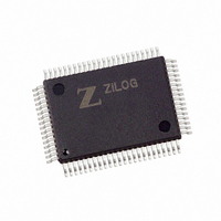
Z16F2811FI20SG Zilog, Z16F2811FI20SG Datasheet - Page 275

Z16F2811FI20SG
Manufacturer Part Number
Z16F2811FI20SG
Description
IC ZNEO MCU FLASH 128K 80QFP
Manufacturer
Zilog
Series
Encore!® ZNEOr
Specifications of Z16F2811FI20SG
Core Processor
ZNEO
Core Size
16-Bit
Speed
20MHz
Connectivity
EBI/EMI, I²C, IrDA, LIN, SPI, UART/USART
Peripherals
Brown-out Detect/Reset, DMA, POR, PWM, WDT
Number Of I /o
60
Program Memory Size
128KB (128K x 8)
Program Memory Type
FLASH
Ram Size
4K x 8
Voltage - Supply (vcc/vdd)
2.7 V ~ 3.6 V
Data Converters
A/D 12x10b
Oscillator Type
Internal
Operating Temperature
0°C ~ 70°C
Package / Case
80-BQFP
Processor Series
Z16F2x
Core
Zneo
Data Bus Width
16 bit
Data Ram Size
4 B
Interface Type
ESPI, I2C, UART
Maximum Clock Frequency
20 MHz
Number Of Programmable I/os
60
Number Of Timers
4
Operating Supply Voltage
2.7 V to 3.6 V
Maximum Operating Temperature
+ 70 C
Mounting Style
SMD/SMT
Development Tools By Supplier
Z16F2800100ZCOG
Minimum Operating Temperature
0 C
On-chip Adc
10 bit, 12 Channel
For Use With
770-1003 - ISP 4PORT FOR ZILOG ZNEO MCU269-4537 - DEV KIT FOR Z16F ZNEO
Lead Free Status / RoHS Status
Lead free / RoHS Compliant
Eeprom Size
-
Lead Free Status / Rohs Status
Details
Other names
269-4534
Available stocks
Company
Part Number
Manufacturer
Quantity
Price
Company:
Part Number:
Z16F2811FI20SG
Manufacturer:
Zilog
Quantity:
155
- Current page: 275 of 388
- Download datasheet (22Mb)
Operation
PS022008-0810
Caution:
Flash Read Protection
Timing Using the Flash Frequency Register
FFREQ[15:0]
Table 134. ZNEO Z16F Series Information Area Map
The Flash Controller provides the proper signals and timing for Word programming, Page
Erase, and Mass erase of the flash memory. The Flash Controller contains a protection
mechanism, using the flash command register (FCMD), to prevent accidental
programming or erasure. The following subsections provide details on the various
operations (Lock, Unlock, Sector Protect, Byte Programming, Page Erase, and Mass
Erase).
Before performing a program or erase operation on the Flash memory, you must first
configure the Flash Frequency register. The Flash Frequency register allows programming
and erasure of the Flash with system clock frequencies ranging from 32 kHz through
20 MHz (the valid range is limited to the device operating frequencies).
The 16-bit Flash Frequency register must be written with the system clock frequency in
kHz before a program or erase operation is initiated. This value is calculated using the
following equation:
Flash programming and erasure is not supported for system clock frequencies
below 32 kHz, above 20 MHz, or outside of the device operating frequency range.
The Flash Frequency register must be loaded with the correct value to ensure prop-
er Flash programming and erase operations.
The user code within the Flash memory is protected from external access.
Programming the Flash Read Protect option bit prevents reading of user code by the
Program Memory Address (Hex)
000000H-00003FH
000040H-000053H
000054H-00007FH
=
System Clock Frequency (Hz)
--------------------------------------------------------------------------- -
P R E L I M I N A R Y
1000
Function
Reserved.
Part Number
20-character ASCII alphanumeric code
Left justified and padded with zeros.
Reserved.
Product Specification
ZNEO
Flash Memory
Z16F Series
259
Related parts for Z16F2811FI20SG
Image
Part Number
Description
Manufacturer
Datasheet
Request
R

Part Number:
Description:
High Performance Microcontrollers
Manufacturer:
ZiLOG Semiconductor
Datasheet:

Part Number:
Description:
Communication Controllers, ZILOG INTELLIGENT PERIPHERAL CONTROLLER (ZIP)
Manufacturer:
Zilog, Inc.
Datasheet:

Part Number:
Description:
KIT DEV FOR Z8 ENCORE 16K TO 64K
Manufacturer:
Zilog
Datasheet:

Part Number:
Description:
KIT DEV Z8 ENCORE XP 28-PIN
Manufacturer:
Zilog
Datasheet:

Part Number:
Description:
DEV KIT FOR Z8 ENCORE 8K/4K
Manufacturer:
Zilog
Datasheet:

Part Number:
Description:
KIT DEV Z8 ENCORE XP 28-PIN
Manufacturer:
Zilog
Datasheet:

Part Number:
Description:
DEV KIT FOR Z8 ENCORE 4K TO 8K
Manufacturer:
Zilog
Datasheet:

Part Number:
Description:
CMOS Z8 microcontroller. ROM 16 Kbytes, RAM 256 bytes, speed 16 MHz, 32 lines I/O, 3.0V to 5.5V
Manufacturer:
Zilog, Inc.
Datasheet:

Part Number:
Description:
Low-cost microcontroller. 512 bytes ROM, 61 bytes RAM, 8 MHz
Manufacturer:
Zilog, Inc.
Datasheet:

Part Number:
Description:
Z8 4K OTP Microcontroller
Manufacturer:
Zilog, Inc.
Datasheet:

Part Number:
Description:
CMOS SUPER8 ROMLESS MCU
Manufacturer:
Zilog, Inc.
Datasheet:

Part Number:
Description:
SL1866 CMOSZ8 OTP Microcontroller
Manufacturer:
Zilog, Inc.
Datasheet:

Part Number:
Description:
SL1866 CMOSZ8 OTP Microcontroller
Manufacturer:
Zilog, Inc.
Datasheet:

Part Number:
Description:
OTP (KB) = 1, RAM = 125, Speed = 12, I/O = 14, 8-bit Timers = 2, Comm Interfaces Other Features = Por, LV Protect, Voltage = 4.5-5.5V
Manufacturer:
Zilog, Inc.
Datasheet:


