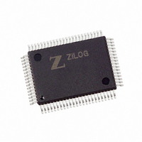
Z16F2811FI20SG Zilog, Z16F2811FI20SG Datasheet - Page 263

Z16F2811FI20SG
Manufacturer Part Number
Z16F2811FI20SG
Description
IC ZNEO MCU FLASH 128K 80QFP
Manufacturer
Zilog
Series
Encore!® ZNEOr
Specifications of Z16F2811FI20SG
Core Processor
ZNEO
Core Size
16-Bit
Speed
20MHz
Connectivity
EBI/EMI, I²C, IrDA, LIN, SPI, UART/USART
Peripherals
Brown-out Detect/Reset, DMA, POR, PWM, WDT
Number Of I /o
60
Program Memory Size
128KB (128K x 8)
Program Memory Type
FLASH
Ram Size
4K x 8
Voltage - Supply (vcc/vdd)
2.7 V ~ 3.6 V
Data Converters
A/D 12x10b
Oscillator Type
Internal
Operating Temperature
0°C ~ 70°C
Package / Case
80-BQFP
Processor Series
Z16F2x
Core
Zneo
Data Bus Width
16 bit
Data Ram Size
4 B
Interface Type
ESPI, I2C, UART
Maximum Clock Frequency
20 MHz
Number Of Programmable I/os
60
Number Of Timers
4
Operating Supply Voltage
2.7 V to 3.6 V
Maximum Operating Temperature
+ 70 C
Mounting Style
SMD/SMT
Development Tools By Supplier
Z16F2800100ZCOG
Minimum Operating Temperature
0 C
On-chip Adc
10 bit, 12 Channel
For Use With
770-1003 - ISP 4PORT FOR ZILOG ZNEO MCU269-4537 - DEV KIT FOR Z16F ZNEO
Lead Free Status / RoHS Status
Lead free / RoHS Compliant
Eeprom Size
-
Lead Free Status / Rohs Status
Details
Other names
269-4534
Available stocks
Company
Part Number
Manufacturer
Quantity
Price
Company:
Part Number:
Z16F2811FI20SG
Manufacturer:
Zilog
Quantity:
155
- Current page: 263 of 388
- Download datasheet (22Mb)
Table 122. ADC0 Control Register 0 (ADC0CTL)
BITS
FIELD
RESET
R/W
ADDR
PS022008-0810
Bit Position
[7]
START0
[6]
CVTRD0
[5]
REFEN
[4]
ADC0EN
[3:0]
ANAIN0
ADC0 Control Register 0
START0
R/W1
7
0
Value (H) Description
The ADC0 Control register initiates the A/D conversion and provides ADC0 status
information.
0000
0001
0010
0
1
0
1
0
1
0
1
CVTRD0
R/W
ADC0 Start / Busy
Writing to 0 has no effect.
Reading a 0 indicates the ADC0 is available to begin a conversion.
Writing to 1 starts a conversion on ADC0.
Reading a 1 indicates a conversion is currently in progress.
Convert On Read
The ADC0 operates normally.
If this bit is set to one, whenever the ADC0D register is read it increments the
ANAIN field by one and start a new conversion. The ANAIN field incr ements
until it r eaches the value set in the ADC0MAX re
conversion on the channel specified by the ADC0MAX register, the next read
resets the ANAIN field to zero. This function is used with the DMA to perform
continuous conversions.
Reference Enable
Internal reference voltage is disabled allowing an external reference voltage to
be used by the ADC0.
Internal reference voltage for the ADC0 is enabled. The internal reference
voltage is measured on the VREF pin.
ADC0 Enable
ADC0 is disabled for low power operation.
ADC0 is enabled for normal use.
Analog Input Select
ANA0 input is selected for analog-to-digital conversion.
ANA1 input is selected for analog-to-digital conversion.
ANA2 input is selected for analog-to-digital conversion.
6
0
REFEN
R/W
5
0
P R E L I M I N A R Y
ADC0EN
R/W
4
0
FF-E500H
R/W
3
0
R/W
2
0
ANAIN0[3:0]
Product Specification
gister. After doing the
ZNEO
R/W
1
0
Analog Functions
Z16F Series
R/W
0
0
247
Related parts for Z16F2811FI20SG
Image
Part Number
Description
Manufacturer
Datasheet
Request
R

Part Number:
Description:
High Performance Microcontrollers
Manufacturer:
ZiLOG Semiconductor
Datasheet:

Part Number:
Description:
Communication Controllers, ZILOG INTELLIGENT PERIPHERAL CONTROLLER (ZIP)
Manufacturer:
Zilog, Inc.
Datasheet:

Part Number:
Description:
KIT DEV FOR Z8 ENCORE 16K TO 64K
Manufacturer:
Zilog
Datasheet:

Part Number:
Description:
KIT DEV Z8 ENCORE XP 28-PIN
Manufacturer:
Zilog
Datasheet:

Part Number:
Description:
DEV KIT FOR Z8 ENCORE 8K/4K
Manufacturer:
Zilog
Datasheet:

Part Number:
Description:
KIT DEV Z8 ENCORE XP 28-PIN
Manufacturer:
Zilog
Datasheet:

Part Number:
Description:
DEV KIT FOR Z8 ENCORE 4K TO 8K
Manufacturer:
Zilog
Datasheet:

Part Number:
Description:
CMOS Z8 microcontroller. ROM 16 Kbytes, RAM 256 bytes, speed 16 MHz, 32 lines I/O, 3.0V to 5.5V
Manufacturer:
Zilog, Inc.
Datasheet:

Part Number:
Description:
Low-cost microcontroller. 512 bytes ROM, 61 bytes RAM, 8 MHz
Manufacturer:
Zilog, Inc.
Datasheet:

Part Number:
Description:
Z8 4K OTP Microcontroller
Manufacturer:
Zilog, Inc.
Datasheet:

Part Number:
Description:
CMOS SUPER8 ROMLESS MCU
Manufacturer:
Zilog, Inc.
Datasheet:

Part Number:
Description:
SL1866 CMOSZ8 OTP Microcontroller
Manufacturer:
Zilog, Inc.
Datasheet:

Part Number:
Description:
SL1866 CMOSZ8 OTP Microcontroller
Manufacturer:
Zilog, Inc.
Datasheet:

Part Number:
Description:
OTP (KB) = 1, RAM = 125, Speed = 12, I/O = 14, 8-bit Timers = 2, Comm Interfaces Other Features = Por, LV Protect, Voltage = 4.5-5.5V
Manufacturer:
Zilog, Inc.
Datasheet:


