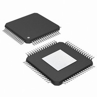
PIC24FJ256DA206-I/PT Microchip Technology, PIC24FJ256DA206-I/PT Datasheet - Page 317

PIC24FJ256DA206-I/PT
Manufacturer Part Number
PIC24FJ256DA206-I/PT
Description
MCU PIC 16BIT FLASH 256K 64TQFP
Manufacturer
Microchip Technology
Series
PIC® 24Fr
Specifications of PIC24FJ256DA206-I/PT
Core Size
16-Bit
Program Memory Size
256KB (85.5K x 24)
Core Processor
PIC
Speed
32MHz
Connectivity
I²C, IrDA, SPI, UART/USART, USB OTG
Peripherals
Brown-out Detect/Reset, GFX, LVD, POR, PWM, WDT
Number Of I /o
52
Program Memory Type
FLASH
Ram Size
96K x 8
Voltage - Supply (vcc/vdd)
2.2 V ~ 3.6 V
Data Converters
A/D 16x10b
Oscillator Type
Internal
Operating Temperature
-40°C ~ 85°C
Package / Case
64-TFQFP
Controller Family/series
PIC24
No. Of I/o's
52
Ram Memory Size
96KB
Cpu Speed
32MHz
No. Of Timers
5
Interface
I2C, SPI, UART, USB
Embedded Interface Type
I2C, SPI, UART, USB
Rohs Compliant
Yes
Lead Free Status / RoHS Status
Lead free / RoHS Compliant
Eeprom Size
-
Lead Free Status / RoHS Status
Lead free / RoHS Compliant, Lead free / RoHS Compliant
Available stocks
Company
Part Number
Manufacturer
Quantity
Price
Company:
Part Number:
PIC24FJ256DA206-I/PT
Manufacturer:
AMD
Quantity:
2 100
Company:
Part Number:
PIC24FJ256DA206-I/PT
Manufacturer:
Microchip Technology
Quantity:
10 000
- Current page: 317 of 408
- Download datasheet (4Mb)
REGISTER 22-21: G1ACTDA: ACTIVE DISPLAY AREA REGISTER
REGISTER 22-22: G1HSYNC: HORIZONTAL SYNCHRONIZATION CONTROL REGISTER
2010 Microchip Technology Inc.
bit 15
bit 7
Legend:
R = Readable bit
-n = Value at POR
bit 15-8
bit 7-0
bit 15
bit 7
Legend:
R = Readable bit
-n = Value at POR
bit 15-8
bit 7-0
ACTLINE7
ACTPIX7
HSLEN7
HSST7
R/W-0
R/W-0
R/W-0
R/W-0
HSLEN<7:0>: HSYNC Pulse-Width Configuration bits (in DISPCLKs)
DPHSOE bit (G1CON3<0>) must be set for the HSYNC signal to toggle; minimum value is 1.
HSST<7:0>: HSYNC Start Delay Configuration bits (in DISPCLKs)
This is the number of DISPCLK cycles from the start of horizontal blanking to the start of HSYNC active.
ACTLINE<7:0>: Number of Lines Before the First Active (Displayed) Line bits
Typically, ACTLINEx = VENSTx (G1DBLCON<15:8>).
This register is added for versatility in the timing of the active lines.
For TFT mode, DPMODE bits (G1CON2<2:0>) = 001; the minimum value is 2.
For STN mode, DPMODE bits (G1CON2<2:0>) = 010,011,100; the minimum value is 0.
ACTPIX<7:0>: Number of Pixels Before the First Active (Displayed) Pixel bits (in DISPCLKs)
Typically, ACTPIXx = HENSTx (G1DBLCON<7:0>).
This register is added for versatility in the timing of the active pixels. Note that the programmed value
is computed in DISPCLK cycles. This value is dependent on the DPGWDTH bit (G1CON2<15:14>).
Refer to the “PIC24F Family Reference Manual”, Section 43. “Graphics Controller Module (GFX)”
for details.
ACTLINE6
HSLEN6
ACTPIX6
HSST6
R/W-0
R/W-0
R/W-0
R/W-0
W = Writable bit
‘1’ = Bit is set
W = Writable bit
‘1’ = Bit is set
ACTLINE5
HSLEN5
ACTPIX5
HSST5
R/W-0
R/W-0
R/W-0
R/W-0
HSLEN4
PIC24FJ256DA210 FAMILY
ACTLINE4
HSST4
R/W-0
R/W-0
ACTPIX4
R/W-0
R/W-0
U = Unimplemented bit, read as ‘0’
‘0’ = Bit is cleared
U = Unimplemented bit, read as ‘0’
‘0’ = Bit is cleared
HSLEN3
HSST3
R/W-0
R/W-0
ACTLINE3
ACTPIX3
R/W-0
R/W-0
HSLEN2
HSST2
R/W-0
R/W-0
ACTLINE2
ACTPIX2
R/W-0
R/W-0
x = Bit is unknown
HSLEN1
x = Bit is unknown
HSST1
ACTLINE1
R/W-0
R/W-0
ACTPIX1
R/W-0
R/W-0
DS39969B-page 317
ACTLINE0
HSLEN0
ACTPIX0
HSST0
R/W-0
R/W-0
R/W-0
R/W-0
bit 8
bit 0
bit 8
bit 0
Related parts for PIC24FJ256DA206-I/PT
Image
Part Number
Description
Manufacturer
Datasheet
Request
R

Part Number:
Description:
Manufacturer:
Microchip Technology Inc.
Datasheet:

Part Number:
Description:
Manufacturer:
Microchip Technology Inc.
Datasheet:

Part Number:
Description:
Manufacturer:
Microchip Technology Inc.
Datasheet:

Part Number:
Description:
Manufacturer:
Microchip Technology Inc.
Datasheet:

Part Number:
Description:
Manufacturer:
Microchip Technology Inc.
Datasheet:

Part Number:
Description:
Manufacturer:
Microchip Technology Inc.
Datasheet:

Part Number:
Description:
Manufacturer:
Microchip Technology Inc.
Datasheet:

Part Number:
Description:
Manufacturer:
Microchip Technology Inc.
Datasheet:


