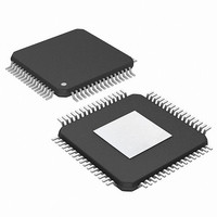
PIC24FJ256DA206-I/PT Microchip Technology, PIC24FJ256DA206-I/PT Datasheet - Page 332

PIC24FJ256DA206-I/PT
Manufacturer Part Number
PIC24FJ256DA206-I/PT
Description
MCU PIC 16BIT FLASH 256K 64TQFP
Manufacturer
Microchip Technology
Series
PIC® 24Fr
Specifications of PIC24FJ256DA206-I/PT
Core Size
16-Bit
Program Memory Size
256KB (85.5K x 24)
Core Processor
PIC
Speed
32MHz
Connectivity
I²C, IrDA, SPI, UART/USART, USB OTG
Peripherals
Brown-out Detect/Reset, GFX, LVD, POR, PWM, WDT
Number Of I /o
52
Program Memory Type
FLASH
Ram Size
96K x 8
Voltage - Supply (vcc/vdd)
2.2 V ~ 3.6 V
Data Converters
A/D 16x10b
Oscillator Type
Internal
Operating Temperature
-40°C ~ 85°C
Package / Case
64-TFQFP
Controller Family/series
PIC24
No. Of I/o's
52
Ram Memory Size
96KB
Cpu Speed
32MHz
No. Of Timers
5
Interface
I2C, SPI, UART, USB
Embedded Interface Type
I2C, SPI, UART, USB
Rohs Compliant
Yes
Lead Free Status / RoHS Status
Lead free / RoHS Compliant
Eeprom Size
-
Lead Free Status / RoHS Status
Lead free / RoHS Compliant, Lead free / RoHS Compliant
Available stocks
Company
Part Number
Manufacturer
Quantity
Price
Company:
Part Number:
PIC24FJ256DA206-I/PT
Manufacturer:
AMD
Quantity:
2 100
Company:
Part Number:
PIC24FJ256DA206-I/PT
Manufacturer:
Microchip Technology
Quantity:
10 000
- Current page: 332 of 408
- Download datasheet (4Mb)
PIC24FJ256DA210 FAMILY
REGISTER 23-7:
EQUATION 23-1:
DS39969B-page 332
bit 15
bit 7
Legend:
R = Readable bit
-n = Value at POR
bit 15-12
bit 11
bit 10
bit 9
bit 8
bit 7-0
Note 1:
CSSL23
R/W-0
U-0
—
(1)
Unimplemented in 64-pin devices, read as ‘0’.
Unimplemented: Read as ‘0’
CSSL27: A/D Input Band Gap Scan Selection bit
1 = Band gap divided-by-six reference (V
0 = Analog channel is omitted from input scan
CSSL26: A/D Input Band Gap Scan Selection bit
1 = Internal core voltage (V
0 = Analog channel is omitted from input scan
CSSL25: A/D Input Half Band Gap Scan Selection bit
1 = Band gap reference (V
0 = Analog channel is omitted from input scan
CSSL24: A/D Input Band Gap Scan Selection bit
1 = Band gap divided-by-two reference (V
0 = Analog channel is omitted from input scan
CSSL<23:16>: Analog Input Pin Scan Selection bits
1 = Corresponding analog channel selected for input scan
0 = Analog channel is omitted from input scan
CSSL22
Note 1:
R/W-0
U-0
—
AD1CSSH: A/D INPUT SCAN SELECT REGISTER (HIGH)
A/D CONVERSION CLOCK PERIOD
(1)
Based on T
W = Writable bit
‘1’ = Bit is set
CSSL21
R/W-0
U-0
—
(1)
CY
BG
= 2 * T
CAP
) is selected for input scan
CSSL20
) is selected for input scan
T
AD
R/W-0
U-0
OSC
ADCS =
—
= T
; Doze mode and PLL are disabled.
CY
(1)
BG
• (ADCS = 1)
BG
T
T
U = Unimplemented bit, read as ‘0’
‘0’ = Bit is cleared
/6) is selected for input scan
AD
CY
/2) is selected for input scan
CSSL19
CSSL27
R/W-0
R/W-0
– 1
(1)
(1)
(1)
CSSL18
CSSL26
R/W-0
R/W-0
(1)
2010 Microchip Technology Inc.
x = Bit is unknown
CSSL17
CSSL25
R/W-0
R/W-0
(1)
CSSL16
CSSL24
R/W-0
R/W-0
bit 8
bit 0
(1)
Related parts for PIC24FJ256DA206-I/PT
Image
Part Number
Description
Manufacturer
Datasheet
Request
R

Part Number:
Description:
Manufacturer:
Microchip Technology Inc.
Datasheet:

Part Number:
Description:
Manufacturer:
Microchip Technology Inc.
Datasheet:

Part Number:
Description:
Manufacturer:
Microchip Technology Inc.
Datasheet:

Part Number:
Description:
Manufacturer:
Microchip Technology Inc.
Datasheet:

Part Number:
Description:
Manufacturer:
Microchip Technology Inc.
Datasheet:

Part Number:
Description:
Manufacturer:
Microchip Technology Inc.
Datasheet:

Part Number:
Description:
Manufacturer:
Microchip Technology Inc.
Datasheet:

Part Number:
Description:
Manufacturer:
Microchip Technology Inc.
Datasheet:


