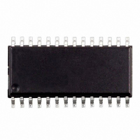
ST72C215G2M6 STMicroelectronics, ST72C215G2M6 Datasheet - Page 100

ST72C215G2M6
Manufacturer Part Number
ST72C215G2M6
Description
IC MCU 8BIT 8K FLASH SOIC-28
Manufacturer
STMicroelectronics
Series
ST7r
Datasheets
1.INDART-ST72C254.pdf
(3 pages)
2.ST72C104G1M6.pdf
(141 pages)
3.ST72C215G2M6.pdf
(140 pages)
Specifications of ST72C215G2M6
Core Processor
ST7
Core Size
8-Bit
Speed
16MHz
Connectivity
SPI
Peripherals
LVD, POR, PWM, WDT
Number Of I /o
22
Program Memory Size
8KB (8K x 8)
Program Memory Type
FLASH
Ram Size
256 x 8
Voltage - Supply (vcc/vdd)
3.2 V ~ 5.5 V
Data Converters
A/D 6x8b
Oscillator Type
Internal
Operating Temperature
-40°C ~ 85°C
Package / Case
28-SOIC (7.5mm Width)
Controller Family/series
ST7
No. Of I/o's
22
Ram Memory Size
256Byte
Cpu Speed
8MHz
No. Of Timers
2
Rohs Compliant
Yes
Processor Series
ST72C2x
Core
ST7
Data Bus Width
8 bit
Data Ram Size
256 B
Interface Type
SPI
Maximum Clock Frequency
16 MHz
Number Of Programmable I/os
22
Number Of Timers
3 bit
Operating Supply Voltage
3.2 V to 5.5 V
Maximum Operating Temperature
+ 85 C
Mounting Style
SMD/SMT
Development Tools By Supplier
ST7MDT1-DVP2/US
Minimum Operating Temperature
- 40 C
On-chip Adc
8 bit
Lead Free Status / RoHS Status
Lead free / RoHS Compliant
Eeprom Size
-
Lead Free Status / Rohs Status
In Transition
Available stocks
Company
Part Number
Manufacturer
Quantity
Price
Company:
Part Number:
ST72C215G2M6
Manufacturer:
ST
Quantity:
2 355
Part Number:
ST72C215G2M6
Manufacturer:
ST
Quantity:
20 000
ST72104G, ST72215G, ST72216G, ST72254G
OPERATING CONDITIONS (Cont’d)
14.3.2 Operating Conditions with Low Voltage Detector (LVD)
Subject to general operating conditions for V
Figure 53. High LVD Threshold Versus V
Figure 54. Medium LVD Threshold Versus V
Figure 55. Low LVD Threshold Versus V
Notes:
1. LVD typical data are based on T
2. Data based on characterization results, not tested in production.
3. The V
4. If the low LVD threshold is selected, when V
anteed to continue functioning until it goes into reset state. The specified V
on phase, but during a power down phase or voltage drop the device will function below this min. level.
100/140
V
V
V
Vt
t
g(VDD)
Symbol
DEVICE UNDER
DEVICE UNDER
DEVICE UNDER
IT+
IT-
hyst
POR
IN THIS AREA
IN THIS AREA
IN THIS AREA
DD
RESET
RESET
RESET
rise time rate condition is needed to insure a correct device power-on and LVD reset. Not tested in production.
Reset release threshold
(V
Reset generation threshold
(V
LVD voltage threshold hysteresis
V
Filtered glitch delay on V
DD
DD
DD
rise time rate
f
f
f
rise)
fall)
OSC
OSC
OSC
12
12
16
12
16
16
8
0
8
0
8
0
[MHz]
[MHz]
[MHz]
2.5
2.5
2.5
Parameter
3)
V
IT-
A
FUNCTIONALITY AND RESET NOT GUARANTEED IN THIS AREA
FUNCTIONALITY AND RESET NOT GUARANTEED IN THIS AREA
=25°C. They are given only as design guidelines and are not tested.
3
3
3V
DD
FUNCTIONALITY NOT GUARANTEED IN THIS AREA
3.2
2)
V
FOR TEMPERATURES HIGHER THAN 85°C
FOR TEMPERATURES HIGHER THAN 85°C
FOR TEMPERATURES HIGHER THAN 85°C
IT-
SEE NOTE 4
DD
3.5
3.5
3.5V
DD
falls below 3.2V, (V
DD
V
High Threshold
Med. Threshold
Low Threshold
High Threshold
Med. Threshold
Low Threshold
V
Not detected by the LVD
DD
IT-
and f
IT+
and f
DD
, f
3.85
-V
OSC
and f
IT-
OSC
OSC
4
4
4
Conditions
, and T
OSC
for FLASH devices
for FLASH devices
4)
for FLASH devices
A
DD
4.5
4.5
4.5
.
minimum operating voltage), the device is guar-
DD
min. value is necessary in the device power
5
5
5
4.10
3.75
3.25
3.85
3.50
3.00
Min
200
0.2
2)4)
3)
2)
2)
2)
2)
2)
3)
5.5
5.5
5.5
Typ
4.30
3.90
3.35
4.05
3.65
3.10
250
SUPPLY VOLTAGE [V]
SUPPLY VOLTAGE [V]
SUPPLY VOLTAGE [V]
1)
FUNCTIONAL AREA
FUNCTIONAL AREA
FUNCTIONAL AREA
FUNCTIONALITY
NOT GUARANTEED
IN THIS AREA
FUNCTIONALITY
NOT GUARANTEED
IN THIS AREA
FUNCTIONALITY
NOT GUARANTEED
IN THIS AREA
Max
4.50
4.05
3.55
4.30
3.95
3.35
300
50
40
V/ms
Unit
mV
ns
V


