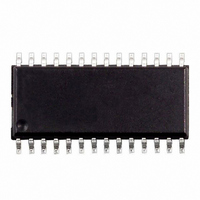
ST72C215G2M6 STMicroelectronics, ST72C215G2M6 Datasheet - Page 127

ST72C215G2M6
Manufacturer Part Number
ST72C215G2M6
Description
IC MCU 8BIT 8K FLASH SOIC-28
Manufacturer
STMicroelectronics
Series
ST7r
Datasheets
1.INDART-ST72C254.pdf
(3 pages)
2.ST72C104G1M6.pdf
(141 pages)
3.ST72C215G2M6.pdf
(140 pages)
Specifications of ST72C215G2M6
Core Processor
ST7
Core Size
8-Bit
Speed
16MHz
Connectivity
SPI
Peripherals
LVD, POR, PWM, WDT
Number Of I /o
22
Program Memory Size
8KB (8K x 8)
Program Memory Type
FLASH
Ram Size
256 x 8
Voltage - Supply (vcc/vdd)
3.2 V ~ 5.5 V
Data Converters
A/D 6x8b
Oscillator Type
Internal
Operating Temperature
-40°C ~ 85°C
Package / Case
28-SOIC (7.5mm Width)
Controller Family/series
ST7
No. Of I/o's
22
Ram Memory Size
256Byte
Cpu Speed
8MHz
No. Of Timers
2
Rohs Compliant
Yes
Processor Series
ST72C2x
Core
ST7
Data Bus Width
8 bit
Data Ram Size
256 B
Interface Type
SPI
Maximum Clock Frequency
16 MHz
Number Of Programmable I/os
22
Number Of Timers
3 bit
Operating Supply Voltage
3.2 V to 5.5 V
Maximum Operating Temperature
+ 85 C
Mounting Style
SMD/SMT
Development Tools By Supplier
ST7MDT1-DVP2/US
Minimum Operating Temperature
- 40 C
On-chip Adc
8 bit
Lead Free Status / RoHS Status
Lead free / RoHS Compliant
Eeprom Size
-
Lead Free Status / Rohs Status
In Transition
Available stocks
Company
Part Number
Manufacturer
Quantity
Price
Company:
Part Number:
ST72C215G2M6
Manufacturer:
ST
Quantity:
2 355
Part Number:
ST72C215G2M6
Manufacturer:
ST
Quantity:
20 000
COMMUNICATION INTERFACE CHARACTERISTICS (Cont’d)
14.11.2 I
Subject to general operating conditions for V
f
Figure 94. Typical Application with I
Notes:
1. Data based on standard I
2. The device must internally provide a hold time of at least 300ns for the SDA signal in order to bridge the undefined
region of the falling edge of SCL.
3. The maximum hold time of the START condition has only to be met if the interface does not stretch the low period of
SCL signal.
4. Measurement points are done at CMOS levels: 0.3xV
t
OSC
w(STO:STA)
Symbol
t
t
t
t
t
w(SCLH)
t
w(SCLL)
su(SDA)
t
su(STO)
t
t
t
su(STA)
t
h(SDA)
h(STA)
r(SDA)
SDA
SCK
r(SCL)
f(SDA)
f(SCL)
I
C
2
, and T
t
C BUS
f(SDA)
b
2
C - Inter IC Control Interface
t
A
SCL clock low time
SCL clock high time
SDA setup time
SDA data hold time
SDA and SCL rise time
SDA and SCL fall time
START condition hold time
Repeated START condition setup time
STOP condition setup time
STOP to START condition time (bus free)
Capacitive load for each bus line
h(STA)
unless otherwise specified.
START
4.7k
t
w(SCKH)
t
r(SDA)
V
2
DD
C protocol requirement, not tested in production.
t
w(SCKL)
Parameter
4.7k
V
DD
t
su(SDA)
2
t
r(SCK)
C Bus and Timing Diagram
100
100
t
h(SDA)
t
DD
f(SCK)
DD
,
SDAI
SCLI
ST72104G, ST72215G, ST72216G, ST72254G
and 0.7xV
Refer to I/O port characteristics for more details on
the input/output alternate function characteristics
(SDAI and SCLI). The ST7 I
requirements of the Standard I
protocol described in the following table.
ST72XXX
Standard mode I
Min
250
0
4.7
4.0
4.0
4.7
4.0
4.7
DD
3)
.
1)
4)
Max
1000
300
400
2
1)
C
t
su(STA)
20+0.1C
20+0.1C
t
su(STO)
Min
100
0
Fast mode I
1.3
0.6
0.6
0.6
0.6
1.3
2
2)
C interface meets the
1)
t
w(STO:STA)
STOP
2
b
b
C communication
REPEATED START
Max
900
300
300
400
2
C
3)
1)
START
127/140
Unit
ms
pF
ns
ns
s
s


