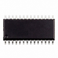
ST72C215G2M6 STMicroelectronics, ST72C215G2M6 Datasheet - Page 117

ST72C215G2M6
Manufacturer Part Number
ST72C215G2M6
Description
IC MCU 8BIT 8K FLASH SOIC-28
Manufacturer
STMicroelectronics
Series
ST7r
Datasheets
1.INDART-ST72C254.pdf
(3 pages)
2.ST72C104G1M6.pdf
(141 pages)
3.ST72C215G2M6.pdf
(140 pages)
Specifications of ST72C215G2M6
Core Processor
ST7
Core Size
8-Bit
Speed
16MHz
Connectivity
SPI
Peripherals
LVD, POR, PWM, WDT
Number Of I /o
22
Program Memory Size
8KB (8K x 8)
Program Memory Type
FLASH
Ram Size
256 x 8
Voltage - Supply (vcc/vdd)
3.2 V ~ 5.5 V
Data Converters
A/D 6x8b
Oscillator Type
Internal
Operating Temperature
-40°C ~ 85°C
Package / Case
28-SOIC (7.5mm Width)
Controller Family/series
ST7
No. Of I/o's
22
Ram Memory Size
256Byte
Cpu Speed
8MHz
No. Of Timers
2
Rohs Compliant
Yes
Processor Series
ST72C2x
Core
ST7
Data Bus Width
8 bit
Data Ram Size
256 B
Interface Type
SPI
Maximum Clock Frequency
16 MHz
Number Of Programmable I/os
22
Number Of Timers
3 bit
Operating Supply Voltage
3.2 V to 5.5 V
Maximum Operating Temperature
+ 85 C
Mounting Style
SMD/SMT
Development Tools By Supplier
ST7MDT1-DVP2/US
Minimum Operating Temperature
- 40 C
On-chip Adc
8 bit
Lead Free Status / RoHS Status
Lead free / RoHS Compliant
Eeprom Size
-
Lead Free Status / Rohs Status
In Transition
Available stocks
Company
Part Number
Manufacturer
Quantity
Price
Company:
Part Number:
ST72C215G2M6
Manufacturer:
ST
Quantity:
2 355
Part Number:
ST72C215G2M6
Manufacturer:
ST
Quantity:
20 000
EMC CHARACTERISTICS (Cont’d)
True Open Drain Pin Protection
The centralized protection (4) is not involved in the
discharge of the ESD stresses applied to true
open drain pads due to the fact that a P-Buffer and
diode to V
local protection between the pad and V
5b) is implemented to completely absorb the posi-
tive ESD discharge.
Figure 75. Positive Stress on a True Open Drain Pad vs. V
Figure 76. Negative Stress on a True Open Drain Pad vs. V
Figure 77. Multisupply Configuration
Main path
Path to avoid
Main path
V
V
DD
DD
SS
are not implemented. An additional
V
V
V
V
SS
SS
DD
DD
V
V
DDA
SSA
(5a)
(3b)
(3b)
(3b)
SS
(5a &
OUT
OUT
ST72104G, ST72215G, ST72216G, ST72254G
BACK TO BACK DIODE
BETWEEN GROUNDS
Multisupply Configuration
When several types of ground (V
power supply (V
reason (better noise immunity...), the structure
shown in
device against ESD.
(4)
(4)
SS
DD
Figure 77
IN
IN
DD
(2b)
, V
is implemented to protect the
DDA
(2b)
(1)
(1)
, ...) are available for any
SS
V
V
(3b)
(5b)
, V
DDA
SSA
SSA
, ...) and
117/140
V
V
V
V
SS
SS
DD
DD


