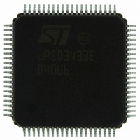
UPSD3433EB40U6 STMicroelectronics, UPSD3433EB40U6 Datasheet - Page 194

UPSD3433EB40U6
Manufacturer Part Number
UPSD3433EB40U6
Description
MCU 8BIT 8032 128KB FLASH 80TQFP
Manufacturer
STMicroelectronics
Series
µPSDr
Datasheet
1.UPSD3434EB40T6.pdf
(293 pages)
Specifications of UPSD3433EB40U6
Core Processor
8032
Core Size
8-Bit
Speed
40MHz
Connectivity
I²C, IrDA, SPI, UART/USART, USB
Peripherals
LVD, POR, PWM, WDT
Number Of I /o
46
Program Memory Size
160KB (160K x 8)
Program Memory Type
FLASH
Ram Size
8K x 8
Voltage - Supply (vcc/vdd)
3 V ~ 5.5 V
Data Converters
A/D 8x10b
Oscillator Type
Internal
Operating Temperature
-40°C ~ 85°C
Package / Case
80-TQFP, 80-VQFP
For Use With
497-5518 - EVAL BOARD RFID READER497-5046 - KIT TOOL FOR ST7/UPSD/STR7 MCU
Lead Free Status / RoHS Status
Lead free / RoHS Compliant
Eeprom Size
-
Other names
497-5660
Available stocks
Company
Part Number
Manufacturer
Quantity
Price
Company:
Part Number:
UPSD3433EB40U6
Manufacturer:
STMicroelectronics
Quantity:
10 000
- Current page: 194 of 293
- Download datasheet (5Mb)
PSD module
28.2.5
Note:
194/293
maintained by alternating between the two flash sectors. For example, a data set of 128
bytes is written and maintained by software in a distributed fashion across one 8K byte
sector of Secondary Flash memory until it becomes full. Then the writing continues on the
other 8K byte sector while erasing the first 8K byte sector. This process repeats
continuously, bouncing back and forth between the two 8K byte sectors. This creates a
wear-leveling effect, which increases the effective number of erase cycles for a data set of
128 bytes to many times more than the base 100K erase cycles of the Flash memory.
EEPROM emulation in Flash memory is typically faster than writing to actual EEPROM
memory, and more reliable because the last known value in a data set is maintained even if
a WRITE cycle is corrupted by a power outage. The EEPROM emulation function can be
called by the user’s firmware, making it appear that the user is writing a single byte, or data
record, thus hiding all of the data management that occurs within the two 8K byte flash
sectors. EEPROM emulation firmware for the uPSD34xx is available from www.st.com/psm.
Alternative mapping schemes
Here are more possible memory maps for the uPSD3433.
Mapping examples would be slightly different for uPSD3433 and uPSD3434, because of the
different sizes of individual Flash memory sectors.
●
●
Figure 66. Mapping: split second Flash in half
Figure 66
Secondary Flash in half, placing two of its sectors into XDATA space and remaining two
sectors into program space. This method allows the designer to put IAP code (or boot
code) into two sectors of Secondary Flash in program space, and use the other two
Secondary Flash sectors for data storage, such as EEPROM emulation in XDATA
space.
Figure 67
maximum code storage, with no Flash memory in XDATA space.
Place the larger Main Flash Memory into program space, but split the
Place both the Main and Secondary Flash memories into program space for
FFFFh
C000h
8000h
2000h
0000h
4000h
Common Memory to All Pages
Common Memory to All Pages
16KB
16KB
Page
fs1
fs0
0
Nothing Mapped
8032 PROGRAM
SPACE (PSEN)
csboot1, 8KB
csboot0, 8KB
16KB
16KB
Page
fs3
fs2
1
16KB
16KB
Page
fs5
fs4
2
16KB
16KB
Page
fs7
fs6
3
8032 XDATA SPACE
csiop, 256B
System I/O
System I/O
(RD and WR)
csboot3
rs0, 8KB
csboot2
Page X
8KB
8KB
AI09174
FFFFh
8000h
6000h
4000h
2100h
2000h
0000h
uPSD34xx
Related parts for UPSD3433EB40U6
Image
Part Number
Description
Manufacturer
Datasheet
Request
R

Part Number:
Description:
MCU 8BIT 8032 128KB FLASH 80TQFP
Manufacturer:
STMicroelectronics
Datasheet:

Part Number:
Description:
MCU 8BIT 8032 128KB FLASH 52TQFP
Manufacturer:
STMicroelectronics
Datasheet:

Part Number:
Description:
STMicroelectronics [RIPPLE-CARRY BINARY COUNTER/DIVIDERS]
Manufacturer:
STMicroelectronics
Datasheet:

Part Number:
Description:
STMicroelectronics [LIQUID-CRYSTAL DISPLAY DRIVERS]
Manufacturer:
STMicroelectronics
Datasheet:

Part Number:
Description:
BOARD EVAL FOR MEMS SENSORS
Manufacturer:
STMicroelectronics
Datasheet:

Part Number:
Description:
NPN TRANSISTOR POWER MODULE
Manufacturer:
STMicroelectronics
Datasheet:

Part Number:
Description:
TURBOSWITCH ULTRA-FAST HIGH VOLTAGE DIODE
Manufacturer:
STMicroelectronics
Datasheet:

Part Number:
Description:
Manufacturer:
STMicroelectronics
Datasheet:

Part Number:
Description:
DIODE / SCR MODULE
Manufacturer:
STMicroelectronics
Datasheet:

Part Number:
Description:
DIODE / SCR MODULE
Manufacturer:
STMicroelectronics
Datasheet:

Part Number:
Description:
Search -----> STE16N100
Manufacturer:
STMicroelectronics
Datasheet:

Part Number:
Description:
Search ---> STE53NA50
Manufacturer:
STMicroelectronics
Datasheet:


