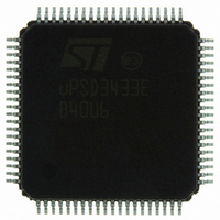
UPSD3433EB40U6 STMicroelectronics, UPSD3433EB40U6 Datasheet - Page 242

UPSD3433EB40U6
Manufacturer Part Number
UPSD3433EB40U6
Description
MCU 8BIT 8032 128KB FLASH 80TQFP
Manufacturer
STMicroelectronics
Series
µPSDr
Datasheet
1.UPSD3434EB40T6.pdf
(293 pages)
Specifications of UPSD3433EB40U6
Core Processor
8032
Core Size
8-Bit
Speed
40MHz
Connectivity
I²C, IrDA, SPI, UART/USART, USB
Peripherals
LVD, POR, PWM, WDT
Number Of I /o
46
Program Memory Size
160KB (160K x 8)
Program Memory Type
FLASH
Ram Size
8K x 8
Voltage - Supply (vcc/vdd)
3 V ~ 5.5 V
Data Converters
A/D 8x10b
Oscillator Type
Internal
Operating Temperature
-40°C ~ 85°C
Package / Case
80-TQFP, 80-VQFP
For Use With
497-5518 - EVAL BOARD RFID READER497-5046 - KIT TOOL FOR ST7/UPSD/STR7 MCU
Lead Free Status / RoHS Status
Lead free / RoHS Compliant
Eeprom Size
-
Other names
497-5660
Available stocks
Company
Part Number
Manufacturer
Quantity
Price
Company:
Part Number:
UPSD3433EB40U6
Manufacturer:
STMicroelectronics
Quantity:
10 000
- Current page: 242 of 293
- Download datasheet (5Mb)
PSD module
Note:
Note:
242/293
●
Non-address signals are still available to PLD inputs and will wake up the PLDs if these
signals are changing state, but will not wake up the memories.
●
●
●
●
●
It is recommended to prevent unused inputs from floating on Ports A, B, C, and D by pulling
them up to V
to achieve this memory standby mode when no inputs are changing—it happens
automatically. Thus, the slower the 8032 clock, the lower the current consumption.
Both PLDs (DPLD and GPLD) are also zero-power, but this is not the default condition.
The 8032 must set a bit in one of the csiop PMMR registers at run-time to achieve zero-
power.
Automatic Power-Down (APD): The APD feature allows the PSD Module to reach its
lowest current consumption levels. If enabled, the APD counter will time-out when there
is a lack of 8032 bus activity for an extended amount of time (8032 asleep). After time-
out occurs, all 8032 address and data buffers on the PSD Module are shut down,
preventing the PSD Module memories and potentially the PLDs from waking up from
standby, even if address inputs are changing state because of noise or any external
components driving the address lines. Since the actual address and data buffers are
turned off, current consumption is even further reduced.
The APD counter requires a relatively slow external clock input on pin PD1 that does
stop when the 8032 goes to sleep mode.
Forced Power-Down (FPD): The MCU can put the PSD Module into Power-Down
mode with the same results as using APD described above, but FPD does not rely on
the APD counter. Instead, FPD will force the PSD Module into Power-Down mode when
the MCU firmware sets a bit in one of the csiop PMMR registers. This is a good
alternative to APD because no external clock is needed for the APD counter.
PSD Module Chip Select Input (CSI): This input on pin PD2 (80-pin devices only) can
be used to disable the internal memories, placing them in standby mode even if
address inputs are changing. This feature does not block any internal signals (the
address and data buffers are still on but signals are ignored) and CSI does not disable
the PLDs. This is a good alternative to using the APD counter, which requires an
external clock on pin PD1.
Non-Turbo Mode: The PLDs can operate in Turbo or non-Turbo modes. Turbo mode
has the shortest signal propagation delay, but consumes more current than non-Turbo
mode. A csiop register can be written by the 8032 to select modes, the default mode is
with Turbo mode enabled. In non-Turbo mode, the PLDs can achieve very low standby
current (~ zero DC current) while no PLD inputs are changing, and the PLDs will even
use less AC current when inputs do change compared to Turbo mode.
When the Turbo mode is enabled, there is a significant DC current component AND the
AC current component is higher than non-Turbo mode, as shown in
page 259
Blocking Bits: Significant power savings can be achieved by blocking 8032 bus control
signals (RD, WR, PSEN, ALE) from reaching PLD inputs, if these signals are not used
in any PLD equations. Blocking is achieved by the 8032 writing to the “blocking bits” in
csiop PMMR registers. Current consumption of the PLDs is directly related to the
composite frequency of all transitions on PLD inputs, so blocking certain PLD inputs
can significantly lower PLD operating frequency and power consumption (resulting in a
lower frequency on the graphs of
SRAM Backup Voltage: Pin PC2 can be configured in PSDsoft to accept an alternate
DC voltage source (battery) to automatically retain the contents of SRAM when V
drops below this alternate voltage.
DD
(5V) and
with a weak external resistor (100K
Figure 97 on page 260
Figure 96 on page 259
(3.3V).
Ω
), or by setting the csiop Direction
and
Figure 97 on page
Figure 96 on
uPSD34xx
260).
DD
Related parts for UPSD3433EB40U6
Image
Part Number
Description
Manufacturer
Datasheet
Request
R

Part Number:
Description:
MCU 8BIT 8032 128KB FLASH 80TQFP
Manufacturer:
STMicroelectronics
Datasheet:

Part Number:
Description:
MCU 8BIT 8032 128KB FLASH 52TQFP
Manufacturer:
STMicroelectronics
Datasheet:

Part Number:
Description:
STMicroelectronics [RIPPLE-CARRY BINARY COUNTER/DIVIDERS]
Manufacturer:
STMicroelectronics
Datasheet:

Part Number:
Description:
STMicroelectronics [LIQUID-CRYSTAL DISPLAY DRIVERS]
Manufacturer:
STMicroelectronics
Datasheet:

Part Number:
Description:
BOARD EVAL FOR MEMS SENSORS
Manufacturer:
STMicroelectronics
Datasheet:

Part Number:
Description:
NPN TRANSISTOR POWER MODULE
Manufacturer:
STMicroelectronics
Datasheet:

Part Number:
Description:
TURBOSWITCH ULTRA-FAST HIGH VOLTAGE DIODE
Manufacturer:
STMicroelectronics
Datasheet:

Part Number:
Description:
Manufacturer:
STMicroelectronics
Datasheet:

Part Number:
Description:
DIODE / SCR MODULE
Manufacturer:
STMicroelectronics
Datasheet:

Part Number:
Description:
DIODE / SCR MODULE
Manufacturer:
STMicroelectronics
Datasheet:

Part Number:
Description:
Search -----> STE16N100
Manufacturer:
STMicroelectronics
Datasheet:

Part Number:
Description:
Search ---> STE53NA50
Manufacturer:
STMicroelectronics
Datasheet:


