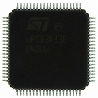
UPSD3433EB40U6 STMicroelectronics, UPSD3433EB40U6 Datasheet - Page 228

UPSD3433EB40U6
Manufacturer Part Number
UPSD3433EB40U6
Description
MCU 8BIT 8032 128KB FLASH 80TQFP
Manufacturer
STMicroelectronics
Series
µPSDr
Datasheet
1.UPSD3434EB40T6.pdf
(293 pages)
Specifications of UPSD3433EB40U6
Core Processor
8032
Core Size
8-Bit
Speed
40MHz
Connectivity
I²C, IrDA, SPI, UART/USART, USB
Peripherals
LVD, POR, PWM, WDT
Number Of I /o
46
Program Memory Size
160KB (160K x 8)
Program Memory Type
FLASH
Ram Size
8K x 8
Voltage - Supply (vcc/vdd)
3 V ~ 5.5 V
Data Converters
A/D 8x10b
Oscillator Type
Internal
Operating Temperature
-40°C ~ 85°C
Package / Case
80-TQFP, 80-VQFP
For Use With
497-5518 - EVAL BOARD RFID READER497-5046 - KIT TOOL FOR ST7/UPSD/STR7 MCU
Lead Free Status / RoHS Status
Lead free / RoHS Compliant
Eeprom Size
-
Other names
497-5660
Available stocks
Company
Part Number
Manufacturer
Quantity
Price
Company:
Part Number:
UPSD3433EB40U6
Manufacturer:
STMicroelectronics
Quantity:
10 000
- Current page: 228 of 293
- Download datasheet (5Mb)
PSD module
28.5.37
Note:
Note:
Note:
Note:
228/293
1
2
1
2
1
2
3
MCU I/O mode
In MCU I/O mode, the 8032 on the MCU Module expands its own I/O by using the I/O Ports
on the PSD Module. The 8032 can read PSD Module I/O pins, set the direction of the I/O
pins, and change the output state of I/O pins by accessing the Data In, Direction, and Data
Out csiop registers respectively at run-time.
To implement MCU I/O mode, each desired pin is specified in PSDsoft Express as MCU I/O
function and given a pin name. Then 8032 firmware is written to set the Direction bit for each
corresponding pin during initialization routines (0 = In, 1 = Out of the chip), then the 8032
firmware simply reads the corresponding Data In register to determine the state of an I/O
pin, or writes to a Data Out register to set the state of a pin. The Direction of each pin may
be changed dynamically by the 8032 if desired. A mixture of input and output pins within a
single port is allowed.
signal paths.
The Data In registers are defined in
defined in
Table 130
Table 122. MCU I/O mode port A data in register
Port A not available on 52-pin uPSD34xx devices
For each bit, 1 = current state of input pin is logic '1,' 0 = current state is logic ’0’
Table 123. MCU I/O mode port B data in register (address = csiop + offset 01h)
For each bit, 1 = current state of input pin is logic '1,' 0 = current state is logic ’0’
Table 124. MCU I/O mode port C data in register (address = csiop + offset 10h)
X = Not guaranteed value, can be read either '1' or '0.'
For each bit, 1 = current state of input pin is logic '1,' 0 = current state is logic ’0’
Table 125. MCU I/O mode port D Data in register (address = csiop + offset 11h)
X = Not guaranteed value, can be read either '1' or '0.'
For each bit, 1 = current state of input pin is logic '1,' 0 = current state is logic ’0’
Not available on 52-pin uPSD34xx devices
Bit 7
Bit 7
Bit 7
Bit 7
PC7
PB7
PA7
X
to
Table 126
Table 133 on page
Bit 6
Bit 6
Bit 6
Bit 6
PB6
PA6
X
X
to
Figure 80 on page 226
Table 129 on page
Bit 5
Bit 5
Bit 5
Bit 5
PB5
PA5
X
X
230.
Table 122
Bit 4
Bit 4
Bit 4
Bit 4
PC4
PB4
PA4
X
229. The Direction registers are defined in
shows the Data In, Data Out, and Direction
to
Table
Bit 3
Bit 3
Bit 3
Bit 3
PC3
PB3
PA3
X
(1)
125. The Data Out registers are
(address = csiop + offset 00h)
PD2
Bit 2
Bit 2
Bit 2
Bit 2
PC2
PB2
PA2
(3)
Bit 1
Bit 1
Bit 1
Bit 1
PD1
PB1
PA1
X
uPSD34xx
Bit 0
Bit 0
Bit 0
Bit 0
PB0
PA0
X
X
Related parts for UPSD3433EB40U6
Image
Part Number
Description
Manufacturer
Datasheet
Request
R

Part Number:
Description:
MCU 8BIT 8032 128KB FLASH 80TQFP
Manufacturer:
STMicroelectronics
Datasheet:

Part Number:
Description:
MCU 8BIT 8032 128KB FLASH 52TQFP
Manufacturer:
STMicroelectronics
Datasheet:

Part Number:
Description:
STMicroelectronics [RIPPLE-CARRY BINARY COUNTER/DIVIDERS]
Manufacturer:
STMicroelectronics
Datasheet:

Part Number:
Description:
STMicroelectronics [LIQUID-CRYSTAL DISPLAY DRIVERS]
Manufacturer:
STMicroelectronics
Datasheet:

Part Number:
Description:
BOARD EVAL FOR MEMS SENSORS
Manufacturer:
STMicroelectronics
Datasheet:

Part Number:
Description:
NPN TRANSISTOR POWER MODULE
Manufacturer:
STMicroelectronics
Datasheet:

Part Number:
Description:
TURBOSWITCH ULTRA-FAST HIGH VOLTAGE DIODE
Manufacturer:
STMicroelectronics
Datasheet:

Part Number:
Description:
Manufacturer:
STMicroelectronics
Datasheet:

Part Number:
Description:
DIODE / SCR MODULE
Manufacturer:
STMicroelectronics
Datasheet:

Part Number:
Description:
DIODE / SCR MODULE
Manufacturer:
STMicroelectronics
Datasheet:

Part Number:
Description:
Search -----> STE16N100
Manufacturer:
STMicroelectronics
Datasheet:

Part Number:
Description:
Search ---> STE53NA50
Manufacturer:
STMicroelectronics
Datasheet:


