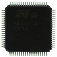
UPSD3433EB40U6 STMicroelectronics, UPSD3433EB40U6 Datasheet - Page 55

UPSD3433EB40U6
Manufacturer Part Number
UPSD3433EB40U6
Description
MCU 8BIT 8032 128KB FLASH 80TQFP
Manufacturer
STMicroelectronics
Series
µPSDr
Datasheet
1.UPSD3434EB40T6.pdf
(293 pages)
Specifications of UPSD3433EB40U6
Core Processor
8032
Core Size
8-Bit
Speed
40MHz
Connectivity
I²C, IrDA, SPI, UART/USART, USB
Peripherals
LVD, POR, PWM, WDT
Number Of I /o
46
Program Memory Size
160KB (160K x 8)
Program Memory Type
FLASH
Ram Size
8K x 8
Voltage - Supply (vcc/vdd)
3 V ~ 5.5 V
Data Converters
A/D 8x10b
Oscillator Type
Internal
Operating Temperature
-40°C ~ 85°C
Package / Case
80-TQFP, 80-VQFP
For Use With
497-5518 - EVAL BOARD RFID READER497-5046 - KIT TOOL FOR ST7/UPSD/STR7 MCU
Lead Free Status / RoHS Status
Lead free / RoHS Compliant
Eeprom Size
-
Other names
497-5660
Available stocks
Company
Part Number
Manufacturer
Quantity
Price
Company:
Part Number:
UPSD3433EB40U6
Manufacturer:
STMicroelectronics
Quantity:
10 000
- Current page: 55 of 293
- Download datasheet (5Mb)
uPSD34xx
13.1
13.1.1
13.1.2
13.1.3
13.1.4
13.1.5
13.1.6
13.1.7
Individual interrupt sources
External interrupts Int0 and Int1
External interrupt inputs on pins EXTINT0 and EXTINT1 (pins 3.2 and 3.3) are either edge-
triggered or level-triggered, depending on bits IT0 and IT1 in the SFR named TCON.
When an external interrupt is generated from an edge-triggered (falling-edge) source, the
appropriate flag bit (IE0 or IE1) is automatically cleared by hardware upon entering the ISR.
When an external interrupt is generated from a level-triggered (low-level) source, the
appropriate flag bit (IE0 or IE1) is NOT automatically cleared by hardware.
Timer 0 and 1 overflow interrupt
Timer 0 and Timer 1 interrupts are generated by the flag bits TF0 and TF1 when there is an
overflow condition in the respective Timer/Counter register (except for Timer 0 in Mode 3).
Timer 2 overflow interrupt
This interrupt is generated to the MCU by a logical OR of flag bits, TF2 and EXE2. The ISR
must read the flag bits to determine the cause of the interrupt.
●
●
UART0 and UART1 interrupt
Each of the UARTs have identical interrupt structure. For each UART, a single interrupt is
generated to the MCU by the logical OR of the flag bits, RI (byte received) and TI (byte
transmitted).
The ISR must read flag bits in the SFR named SCON0 for UART0, or SCON1 for UART1 to
determine the cause of the interrupt.
SPI interrupt
The SPI interrupt has four interrupt sources, which are logically ORed together when
interrupting the MCU. The ISR must read the flag bits to determine the cause of the
interrupt.
A flag bit is set for: end of data transmit (TEISF); data receive overrun (RORISF); transmit
buffer empty (TISF); or receive buffer full (RISF).
I
The flag bit INTR is set by a variety of conditions occurring on the I
own slave address (ADDR flag); received general call address (GC flag); received STOP
condition (STOP flag); or successful transmission or reception of a data byte.The ISR must
read the flag bits to determine the cause of the interrupt.
ADC interrupt
The flag bit AINTF is set when an A-to-D conversion has completed.
2
C interrupt
TF2 is set by an overflow of Timer 2.
EXE2 is generated by the falling edge of a signal on the external pin, T2X (pin P1.1).
2
C interface: received
Interrupt system
55/293
Related parts for UPSD3433EB40U6
Image
Part Number
Description
Manufacturer
Datasheet
Request
R

Part Number:
Description:
MCU 8BIT 8032 128KB FLASH 80TQFP
Manufacturer:
STMicroelectronics
Datasheet:

Part Number:
Description:
MCU 8BIT 8032 128KB FLASH 52TQFP
Manufacturer:
STMicroelectronics
Datasheet:

Part Number:
Description:
STMicroelectronics [RIPPLE-CARRY BINARY COUNTER/DIVIDERS]
Manufacturer:
STMicroelectronics
Datasheet:

Part Number:
Description:
STMicroelectronics [LIQUID-CRYSTAL DISPLAY DRIVERS]
Manufacturer:
STMicroelectronics
Datasheet:

Part Number:
Description:
BOARD EVAL FOR MEMS SENSORS
Manufacturer:
STMicroelectronics
Datasheet:

Part Number:
Description:
NPN TRANSISTOR POWER MODULE
Manufacturer:
STMicroelectronics
Datasheet:

Part Number:
Description:
TURBOSWITCH ULTRA-FAST HIGH VOLTAGE DIODE
Manufacturer:
STMicroelectronics
Datasheet:

Part Number:
Description:
Manufacturer:
STMicroelectronics
Datasheet:

Part Number:
Description:
DIODE / SCR MODULE
Manufacturer:
STMicroelectronics
Datasheet:

Part Number:
Description:
DIODE / SCR MODULE
Manufacturer:
STMicroelectronics
Datasheet:

Part Number:
Description:
Search -----> STE16N100
Manufacturer:
STMicroelectronics
Datasheet:

Part Number:
Description:
Search ---> STE53NA50
Manufacturer:
STMicroelectronics
Datasheet:


