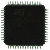
UPSD3433EB40U6 STMicroelectronics, UPSD3433EB40U6 Datasheet - Page 243

UPSD3433EB40U6
Manufacturer Part Number
UPSD3433EB40U6
Description
MCU 8BIT 8032 128KB FLASH 80TQFP
Manufacturer
STMicroelectronics
Series
µPSDr
Datasheet
1.UPSD3434EB40T6.pdf
(293 pages)
Specifications of UPSD3433EB40U6
Core Processor
8032
Core Size
8-Bit
Speed
40MHz
Connectivity
I²C, IrDA, SPI, UART/USART, USB
Peripherals
LVD, POR, PWM, WDT
Number Of I /o
46
Program Memory Size
160KB (160K x 8)
Program Memory Type
FLASH
Ram Size
8K x 8
Voltage - Supply (vcc/vdd)
3 V ~ 5.5 V
Data Converters
A/D 8x10b
Oscillator Type
Internal
Operating Temperature
-40°C ~ 85°C
Package / Case
80-TQFP, 80-VQFP
For Use With
497-5518 - EVAL BOARD RFID READER497-5046 - KIT TOOL FOR ST7/UPSD/STR7 MCU
Lead Free Status / RoHS Status
Lead free / RoHS Compliant
Eeprom Size
-
Other names
497-5660
Available stocks
Company
Part Number
Manufacturer
Quantity
Price
Company:
Part Number:
UPSD3433EB40U6
Manufacturer:
STMicroelectronics
Quantity:
10 000
- Current page: 243 of 293
- Download datasheet (5Mb)
uPSD34xx
Note:
Note:
1
register to “output” at run-time for all unused inputs. This will prevent the CMOS input buffers
of unused input pins from drawing excessive current.
The csiop PMMR register definitions are shown in
page
Table 144. Power management mode register PMMR0 (address = csiop + offset B0h)
All the bits of this register are cleared to zero following Power-up. Subsequent Reset (RST)
pulses do not clear the registers.
Blocking bits should be set to logic ’1’ only if the signal is not needed in a DPLD or GPLD
logic equation.
Bit 0
Bit 1 APD Enable
Bit 2
Bit 3
Bit 4
Bit 5
Bit 6
Bit 7
244.
Blocking Bit,
Blocking Bit,
PLD Turbo
CLKIN to
CLKIN to
PLDs
Disable
Only
OMCs
X
X
X
X
(1)
(1)
0 =
1 =
0 =
1 =
0 =
1 =
on
off
on
off
on
off
0
0
1
0
0
0
Not used, and should be set to zero.
Automatic Power Down (APD) counter is disabled.
APD counter is enabled
Not used, and should be set to zero.
PLD Turbo mode is on
PLD Turbo mode is off, saving power.
CLKIN (pin PD1) to the PLD Input Bus is not blocked. Every transition of
CLKIN powers-up the PLDs.
CLKIN input to PLD Input Bus is blocked, saving power. But CLKIN still
goes to APD counter.
CLKIN input is not blocked from reaching all OMCs’ common clock
inputs.
CLKIN input to common clock of all OMCs is blocked, saving power. But
CLKIN still goes to APD counter and all PLD logic besides the common
clock input on OMCs.
Not used, and should be set to zero.
Not used, and should be set to zero.
Table 144
through
Table 146 on
PSD module
243/293
Related parts for UPSD3433EB40U6
Image
Part Number
Description
Manufacturer
Datasheet
Request
R

Part Number:
Description:
MCU 8BIT 8032 128KB FLASH 80TQFP
Manufacturer:
STMicroelectronics
Datasheet:

Part Number:
Description:
MCU 8BIT 8032 128KB FLASH 52TQFP
Manufacturer:
STMicroelectronics
Datasheet:

Part Number:
Description:
STMicroelectronics [RIPPLE-CARRY BINARY COUNTER/DIVIDERS]
Manufacturer:
STMicroelectronics
Datasheet:

Part Number:
Description:
STMicroelectronics [LIQUID-CRYSTAL DISPLAY DRIVERS]
Manufacturer:
STMicroelectronics
Datasheet:

Part Number:
Description:
BOARD EVAL FOR MEMS SENSORS
Manufacturer:
STMicroelectronics
Datasheet:

Part Number:
Description:
NPN TRANSISTOR POWER MODULE
Manufacturer:
STMicroelectronics
Datasheet:

Part Number:
Description:
TURBOSWITCH ULTRA-FAST HIGH VOLTAGE DIODE
Manufacturer:
STMicroelectronics
Datasheet:

Part Number:
Description:
Manufacturer:
STMicroelectronics
Datasheet:

Part Number:
Description:
DIODE / SCR MODULE
Manufacturer:
STMicroelectronics
Datasheet:

Part Number:
Description:
DIODE / SCR MODULE
Manufacturer:
STMicroelectronics
Datasheet:

Part Number:
Description:
Search -----> STE16N100
Manufacturer:
STMicroelectronics
Datasheet:

Part Number:
Description:
Search ---> STE53NA50
Manufacturer:
STMicroelectronics
Datasheet:


