DS87C550-QCL+ Maxim Integrated Products, DS87C550-QCL+ Datasheet - Page 11
DS87C550-QCL+
Manufacturer Part Number
DS87C550-QCL+
Description
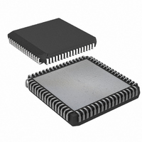
IC MCU EPROM ADC/PWM HS 68-PLCC
Manufacturer
Maxim Integrated Products
Series
87Cr
Datasheet
1.DS87C550-QNL.pdf
(49 pages)
Specifications of DS87C550-QCL+
Core Processor
8051
Core Size
8-Bit
Speed
33MHz
Connectivity
EBI/EMI, SIO, UART/USART
Peripherals
Power-Fail Reset, PWM, WDT
Number Of I /o
55
Program Memory Size
8KB (8K x 8)
Program Memory Type
OTP
Ram Size
1K x 8
Voltage - Supply (vcc/vdd)
4.5 V ~ 5.5 V
Data Converters
A/D 6x10b
Oscillator Type
External
Operating Temperature
0°C ~ 70°C
Package / Case
68-LCC, 68-PLCC
Lead Free Status / RoHS Status
Lead free / RoHS Compliant
Eeprom Size
-


DS87C550 EPROM High-Speed Microcontroller with ADC and PWM
ROM address of 5k. This would cause the current address to switch from internal to external and
potentially cause invalid operation. Similarly, do not instantly switch from external to internal memory.
For example, do not select a maximum ROM address of 8kB from an external ROM address of 7kB (if
ROMSIZE is set for 4kB or less).
Off-chip memory is accessed using the multiplexed address/data bus on P0 and the MSB address on P2.
While serving as a memory bus, these pins are not available as I/O ports. This convention follows the
standard 8051 method of expanding on-chip memory. Off-chip ROM access also occurs if the EA pin is
logic 0. EA overrides all bit settings. The PSEN signal will go active (low) to serve as a chip enable or
output enable when Ports 0 & 2 fetch from external ROM.
ROM MEMORY MAP Figure 2
DATA MEMORY
Unlike many 8051 derivatives, the DS87C550 contains additional on-chip data memory. In addition to
the standard 256 bytes of data RAM accessed by direct instructions, the DS87C550 contains another 1kB
of data memory that is accessed using the MOVX instruction. Although physically on-chip, software
treats this area as though it was located off-chip. The 1kB of SRAM is permanently located from address
0000h to 03FFh (when enabled).
Access to the on-chip data RAM is optional under software control. When enabled by software, the data
SRAM is between 0000h and 03FFh. Any MOVX instruction that uses this area will go to the on-chip
RAM while enabled. MOVX addresses greater than 1kB automatically go to external memory through
Ports 0 & 2.
When disabled, the 1kB memory area is transparent to the system memory map. Any MOVX directed to
the space between 0000h and FFFFh goes to the expanded bus on Ports 0 & 2. This also is the default
condition. This default allows the DS87C550 to drop into an existing system that uses these addresses for
other hardware and still have full compatibility.
The on-chip data area is software selectable using two bits in the Power Management Register (DME1,
DME0). This selection is dynamically programmable. Thus access to the on-chip area becomes
transparent to reach off-chip devices at the same addresses. These bits have the following operation:
11 of 49
Related parts for DS87C550-QCL+
Image
Part Number
Description
Manufacturer
Datasheet
Request
R

Part Number:
Description:
IC MCU EPROM ADC/PWM HS 68-PLCC
Manufacturer:
Maxim Integrated Products
Datasheet:

Part Number:
Description:
Eprom High-speed Microcontroller With Adc And Pwm
Manufacturer:
Maxim Integrated Products, Inc.
Datasheet:

Part Number:
Description:
MAX7528KCWPMaxim Integrated Products [CMOS Dual 8-Bit Buffered Multiplying DACs]
Manufacturer:
Maxim Integrated Products
Datasheet:
Part Number:
Description:
Single +5V, fully integrated, 1.25Gbps laser diode driver.
Manufacturer:
Maxim Integrated Products
Datasheet:
Part Number:
Description:
Single +5V, fully integrated, 155Mbps laser diode driver.
Manufacturer:
Maxim Integrated Products
Datasheet:
Part Number:
Description:
VRD11/VRD10, K8 Rev F 2/3/4-Phase PWM Controllers with Integrated Dual MOSFET Drivers
Manufacturer:
Maxim Integrated Products
Datasheet:
Part Number:
Description:
Highly Integrated Level 2 SMBus Battery Chargers
Manufacturer:
Maxim Integrated Products
Datasheet:
Part Number:
Description:
Current Monitor and Accumulator with Integrated Sense Resistor; ; Temperature Range: -40°C to +85°C
Manufacturer:
Maxim Integrated Products
Part Number:
Description:
TSSOP 14/A°/RS-485 Transceivers with Integrated 100O/120O Termination Resis
Manufacturer:
Maxim Integrated Products
Part Number:
Description:
TSSOP 14/A°/RS-485 Transceivers with Integrated 100O/120O Termination Resis
Manufacturer:
Maxim Integrated Products
Part Number:
Description:
QFN 16/A°/AC-DC and DC-DC Peak-Current-Mode Converters with Integrated Step
Manufacturer:
Maxim Integrated Products
Part Number:
Description:
TDFN/A/65V, 1A, 600KHZ, SYNCHRONOUS STEP-DOWN REGULATOR WITH INTEGRATED SWI
Manufacturer:
Maxim Integrated Products
Part Number:
Description:
Integrated Temperature Controller f
Manufacturer:
Maxim Integrated Products
Part Number:
Description:
SOT23-6/I°/45MHz to 650MHz, Integrated IF VCOs with Differential Output
Manufacturer:
Maxim Integrated Products
Part Number:
Description:
SOT23-6/I°/45MHz to 650MHz, Integrated IF VCOs with Differential Output
Manufacturer:
Maxim Integrated Products