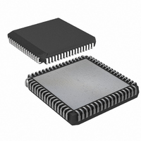
DS87C550-QCL+ Maxim Integrated Products, DS87C550-QCL+ Datasheet - Page 15

DS87C550-QCL+
Manufacturer Part Number
DS87C550-QCL+
Description
IC MCU EPROM ADC/PWM HS 68-PLCC
Manufacturer
Maxim Integrated Products
Series
87Cr
Datasheet
1.DS87C550-QNL.pdf
(49 pages)
Specifications of DS87C550-QCL+
Core Processor
8051
Core Size
8-Bit
Speed
33MHz
Connectivity
EBI/EMI, SIO, UART/USART
Peripherals
Power-Fail Reset, PWM, WDT
Number Of I /o
55
Program Memory Size
8KB (8K x 8)
Program Memory Type
OTP
Ram Size
1K x 8
Voltage - Supply (vcc/vdd)
4.5 V ~ 5.5 V
Data Converters
A/D 6x10b
Oscillator Type
External
Operating Temperature
0°C ~ 70°C
Package / Case
68-LCC, 68-PLCC
Lead Free Status / RoHS Status
Lead free / RoHS Compliant
Eeprom Size
-
cycles. It is important to note the distinction between the system clock and the machine cycle clock as
they are often confused, creating errors in timing calculations. In performing timing calculations, it is
important to remember that all timers and internal peripherals operate off of some version of the system
clock while the instruction execution engine always operates off of the machine cycle clock.
When CD1 and CD0 (PMR.7-6) are both cleared to a logic 0, the multiplexer selects the frequency
multiplier output. The frequency multiplier can supply a clock that is 2 times or 4 times the frequency of
the incoming signal. If the times-4 multiplier is selected by setting the 4X/
example, the incoming signal is multiplied by 4. This 4X clock is then passed through the multiplexer,
and then output to the CPU State Clock Generation circuits. These CPU State Clock Generation circuits
always divide the incoming clock by 4 to arrive at the four states (called a machine cycle) necessary for
correct processor operation. In this example, since the clock multiplier multiplies by four and the CPU
State Clock Generation circuit divides by 4, the apparent instruction execution speed is 1 external (or
crystal oscillator) clock per instruction. If the 4X/
execution speed is 2 clocks per instruction.
It is important to note that the clock multiplier function does not increase the maximum clock (system
clock) rate of the device. The DS87C550 operates at a maximum system clock rate of 33MHz. Therefore,
the maximum crystal frequency is 8.25MHz when a clock multiplier of 4 is used, and is 16.5MHz when a
clock multiplier of 2 is used. The purpose of the clock multiplier is to simplify crystal selection when
maximum processor operation is desired. Specifically, an 8.25MHz fundamental mode, AT cut, parallel
resonant crystal is much easier to obtain than the same crystal at 33MHz. Most crystals in that frequency
range tend to be third overtone type.
As illustrated in Figure 3, the programmable Clock Divide control bits CD1-CD0 (PMR.7-6) provide the
processor with the ability to adapt to different crystal (and external clock) frequencies and also to allow
extreme division of the incoming clock providing lower power operation when desired. The effect of
these bits is shown in Table 5.
CD1:CD0 OPERATION Table 5
Besides the ability to use a multiplied clock signal, the normal mode of operation, i.e. the reset default
condition (CD1 = 1, CD0 = 0) passes the incoming crystal or external oscillator clock signal straight
through as the system clock. Because of the CPU State Clock generation circuitry’s normal divide-by-4
function, the default execution speed of the DS87C550’s basic instruction is one-fourth the clock
frequency.
The selection of instruction cycle rate takes effect after a delay of one machine cycle. Note that the clock
divider choice applies to all functions including timers. Since baud rates are altered, it may be difficult to
conduct serial communication while in divide-by-1024 mode. This is simplified by the use of switchback
mode (described later) included on the DS87C550.
CD1
0
0
1
1
CD0
0
1
0
1
Frequency multiplier (1 or 2 clocks per machine cycle)
Reserved
Clock divided by 4 (4 clocks per machine cycle) Default
Clock divided by 1024 (1024 clocks per machine cycle)
Instruction Execution
15 of 49
2X
bit is set to 0, then the apparent instruction
2X
bit (PMR.3) to 1, for


