DS87C550-QCL+ Maxim Integrated Products, DS87C550-QCL+ Datasheet - Page 4
DS87C550-QCL+
Manufacturer Part Number
DS87C550-QCL+
Description
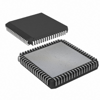
IC MCU EPROM ADC/PWM HS 68-PLCC
Manufacturer
Maxim Integrated Products
Series
87Cr
Datasheet
1.DS87C550-QNL.pdf
(49 pages)
Specifications of DS87C550-QCL+
Core Processor
8051
Core Size
8-Bit
Speed
33MHz
Connectivity
EBI/EMI, SIO, UART/USART
Peripherals
Power-Fail Reset, PWM, WDT
Number Of I /o
55
Program Memory Size
8KB (8K x 8)
Program Memory Type
OTP
Ram Size
1K x 8
Voltage - Supply (vcc/vdd)
4.5 V ~ 5.5 V
Data Converters
A/D 6x10b
Oscillator Type
External
Operating Temperature
0°C ~ 70°C
Package / Case
68-LCC, 68-PLCC
Lead Free Status / RoHS Status
Lead free / RoHS Compliant
Eeprom Size
-


PIN DESCRIPTION Table 1
PLCC/
CLCC
16-23
36
37
15
35
34
47
48
49
16
17
18
19
20
21
22
23
2
10-17
QFP
14
72
34
35
32
31
48
49
50
10
11
12
13
15
16
17
9
SIGNAL NAME
P1.0-P1.7
XTAL1
XTAL2
GND
PSEN
ALE
RST
V
EA
CC
V
GND – Digital ground.
RST - I/O. The RST input pin contains a Schmitt voltage input to recognize
external active high Reset inputs. The pin also employs an internal pulldown
resistor to allow for a combination of wired OR external Reset sources. An RC is
not required for power-up, as the DS87C550 provides this function internally. This
pin also acts as an output when the source of the reset is internal to the device (i.e.,
watchdog timer, power-fail, or crystal-fail detect). In this case, the RST pin will be
held high while the processor is in a Reset state, and will return to low as the
processor exits this state. When this output capability is used, the RST pin should
not be connected to an RC network or a logic output driver.
Input - The crystal oscillator pins XTAL1 and XTAL2 provide support for
fundamental mode, parallel resonant, AT cut crystals. XTAL1 acts also as an input
if there is an external clock source in place of a crystal. XTAL2 serves as the
output of the crystal amplifier. Note that this output cannot be used to drive any
additional load when a crystal is attached as this can disturb the oscillator circuit.
connected to optional external ROM memory as a chip enable. PSEN will provide
an active low pulse during a program byte access, and is driven high when not
accessing external program memory.
ALE - Output. The Address Latch Enable output functions as a clock to latch the
external address LSB from the multiplexed address/data bus on Port 0. This signal
is commonly connected to the latch enable of an external 373 family transparent
latch. ALE is driven high when the DS87C550 is in a Reset condition. ALE can
also be disabled and forced high using the EMI reduction mode ALEOFF.
DS87C550 to use an external program memory. The internal RAM is still
accessible as determined by register settings.
use internal program memory. The input level on this pin is latched at reset.
Port 1 - I/O. Port 1 functions as both an 8-bit, bi-directional I/O port and an
alternate functional interface for several internal resources. The reset condition of
Port 1 is all bits at logic 1. In this state, a weak pullup holds the port high. This
condition allows the pins to serve as both input and output. Input is possible since
any external circuit whose output drives the port will overcome the weak pullup.
When software writes a 0 to any Port 1 pin, the DS87C550 will activate a strong
pulldown that remains on until either a 1 is written or a reset occurs. Writing a 1
after the port has been at 0 will cause a strong transition driver to turn on, followed
by a weaker sustaining pullup. Once the momentary strong driver turns off, the
port again returns to a weakly held high output (and input) state. The alternate
functions of Port 1 pins are detailed below. Note that when the Capture/Compare
functions of timer 2 are used, the interrupt input pins become capture trigger
inputs.
Port
P1.0
P1.1
P1.2
P1.3
P1.4
P1.5
P1.6
P1.7
PSEN
EA
CC
- Input. An active low input pin that when connected to ground will force the
- Digital +5V power input.
- Output. The Program Store Enable output. This signal is commonly
Alternate Function
INT2/CT0 External Interrupt 2/Capture Trigger 0
INT3/CT1 External Interrupt 3/Capture Trigger 1
INT4/CT2 External Interrupt 4/Capture Trigger 2
INT5/CT3 External Interrupt 5/Capture Trigger 3
T2
T2EX
RXD1
TXD1
4 of 49
External I/O for Timer/Counter 2
Timer/Counter 2 Capture/Reload Trigger
Serial Port 1 Input
Serial Port 1 Output
DESCRIPTION
EA
should be connected to V
CC
to
Related parts for DS87C550-QCL+
Image
Part Number
Description
Manufacturer
Datasheet
Request
R

Part Number:
Description:
IC MCU EPROM ADC/PWM HS 68-PLCC
Manufacturer:
Maxim Integrated Products
Datasheet:

Part Number:
Description:
Eprom High-speed Microcontroller With Adc And Pwm
Manufacturer:
Maxim Integrated Products, Inc.
Datasheet:

Part Number:
Description:
MAX7528KCWPMaxim Integrated Products [CMOS Dual 8-Bit Buffered Multiplying DACs]
Manufacturer:
Maxim Integrated Products
Datasheet:
Part Number:
Description:
Single +5V, fully integrated, 1.25Gbps laser diode driver.
Manufacturer:
Maxim Integrated Products
Datasheet:
Part Number:
Description:
Single +5V, fully integrated, 155Mbps laser diode driver.
Manufacturer:
Maxim Integrated Products
Datasheet:
Part Number:
Description:
VRD11/VRD10, K8 Rev F 2/3/4-Phase PWM Controllers with Integrated Dual MOSFET Drivers
Manufacturer:
Maxim Integrated Products
Datasheet:
Part Number:
Description:
Highly Integrated Level 2 SMBus Battery Chargers
Manufacturer:
Maxim Integrated Products
Datasheet:
Part Number:
Description:
Current Monitor and Accumulator with Integrated Sense Resistor; ; Temperature Range: -40°C to +85°C
Manufacturer:
Maxim Integrated Products
Part Number:
Description:
TSSOP 14/A°/RS-485 Transceivers with Integrated 100O/120O Termination Resis
Manufacturer:
Maxim Integrated Products
Part Number:
Description:
TSSOP 14/A°/RS-485 Transceivers with Integrated 100O/120O Termination Resis
Manufacturer:
Maxim Integrated Products
Part Number:
Description:
QFN 16/A°/AC-DC and DC-DC Peak-Current-Mode Converters with Integrated Step
Manufacturer:
Maxim Integrated Products
Part Number:
Description:
TDFN/A/65V, 1A, 600KHZ, SYNCHRONOUS STEP-DOWN REGULATOR WITH INTEGRATED SWI
Manufacturer:
Maxim Integrated Products
Part Number:
Description:
Integrated Temperature Controller f
Manufacturer:
Maxim Integrated Products
Part Number:
Description:
SOT23-6/I°/45MHz to 650MHz, Integrated IF VCOs with Differential Output
Manufacturer:
Maxim Integrated Products
Part Number:
Description:
SOT23-6/I°/45MHz to 650MHz, Integrated IF VCOs with Differential Output
Manufacturer:
Maxim Integrated Products