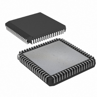
DS87C550-QCL+ Maxim Integrated Products, DS87C550-QCL+ Datasheet - Page 30

DS87C550-QCL+
Manufacturer Part Number
DS87C550-QCL+
Description
IC MCU EPROM ADC/PWM HS 68-PLCC
Manufacturer
Maxim Integrated Products
Series
87Cr
Datasheet
1.DS87C550-QNL.pdf
(49 pages)
Specifications of DS87C550-QCL+
Core Processor
8051
Core Size
8-Bit
Speed
33MHz
Connectivity
EBI/EMI, SIO, UART/USART
Peripherals
Power-Fail Reset, PWM, WDT
Number Of I /o
55
Program Memory Size
8KB (8K x 8)
Program Memory Type
OTP
Ram Size
1K x 8
Voltage - Supply (vcc/vdd)
4.5 V ~ 5.5 V
Data Converters
A/D 6x10b
Oscillator Type
External
Operating Temperature
0°C ~ 70°C
Package / Case
68-LCC, 68-PLCC
Lead Free Status / RoHS Status
Lead free / RoHS Compliant
Eeprom Size
-
The three available priority levels are low, high, and highest. The highest priority level is reserved for the
Power-Fail Interrupt only. All other interrupt priority levels have individual priority bits that when set to a
1 establish the particular interrupt as high priority. In addition to the user selectable priorities, each
interrupt also has an inherent or “natural priority”. Given that all interrupt sources maintain the default
low priority, the natural priority determines the priority of simultaneously occurring interrupts. Table 9
identifies the available interrupt sources and their flags, enables, natural priority, and available priority
selection bits.
INTERRUPT SOURCES AND PRIORITIES Table 9
1
fully enabled.
EPROM PROGRAMMING
The DS87C550 follows 8kB EPROM standards for the 8051 family. It is available in a UV erasable,
ceramic windowed package and in plastic packages for one-time user-programmable versions. The part
has unique signature information so programmers can support its specific EPROM options.
PROGRAMMING PROCEDURE
The DS87C550 should run from a clock speed between 4 and 6MHz when programmed. The
programming fixture should apply address information for each byte to the address lines and the data
value to the data lines. The control signals must be manipulated as shown in Table 10. The diagram in
Figure 5 shows the expected electrical connection for programming. Note that the programmer must
apply addresses in demultiplexed fashion to Ports 1 and 2 with data on Port 0. Waveforms and timing are
provided in the Electrical Specifications.
External interrupts 2/3/4/5 also require the appropriate bits in the CTCON register to be configured before the interrupt is
INT2/CF0
INT3/CF1
INT4/CF2
INT5/CF3
SCON1
SCON0
NAME
CM0F
CM1F
CM2F
INT0
INT1
A/D
TF0
TF1
TF2
PFI
External Interrupt 2 or
External Interrupt 3 or
External Interrupt 4 or
External Interrupt 5 or
TI1 or RI1 from serial
TI0 or RI0 from serial
Power Fail Interrupt
External Interrupt 0
External Interrupt 1
Compare Match 0
Compare Match 1
Compare Match 2
DESCRIPTION
A/D Converter
Capture 0
Capture 1
Capture 2
Capture 3
Interrupt
Timer 0
Timer 1
Timer 2
port 1
port 0
VECTOR
0Bh
1Bh
2Bh
3Bh
4Bh
5Bh
6Bh
7Bh
33h
03h
13h
23h
43h
53h
63h
73h
PRIORITY
NATURAL
30 of 49
10
11
12
13
14
15
0
1
2
3
4
5
6
7
8
9
EOC(ADCON1.6)
IE2/CF0(T2IR.0)
IE3/CF1(T2IR.1)
IE4/CF2(T2IR.2)
IE5/CF3(T2IR.3)
PFI(WDCON.4)
RI_1(SCON1.0)
RI_0(SCON0.0)
TF2B(T2SEL.4)
TI_1(SCON1.1)
TI_0(SCON0.1)
CM0F(T2IR.4)
CM1F(T2IR.5)
CM2F(T2IR.6)
IEO(TCON.1)
TF0(TCON.5)
TF1(TCON.7)
TF2(TCON.7)
IE1(TCON.3)
FLAG
BIT
EX3/EC1(EIE.1)
EX4/EC2(EIE.2)
EX5/EC3(EIE.3)
EPFI(WDCON.5)
EX2/EC0(EIE.0)
ECM0(EIE.4)
ECM1(EIE.5)
ECM2(EIE.6)
ET2(EIE.7)
EAD(IE.6)
EX0(IE.0)
EX1(IE.2)
ENABLE
ET0(IE.1)
ET1(IE.3)
ES1(IE.5)
ES0(IE.4)
BIT
1
1
1
1
CONTROL BIT
PX2/PC0(EIP.0)
PX3/PC1(EIP.1)
PX4/PC2(EIP.2)
PX5/PC3(EIP.3)
PCM0(EIP.4)
PCM1(EIP.5)
PCM2(EIP.6)
PRIORITY
PT2(EIP.7)
PAD(IP.6)
PX0(IP.0)
PX1(IP.2)
PS1(IP.5)
PT0(IP.1)
PT1(IP.3)
PS0(IP.4)
N/A


