CYWUSB6934-28SEC Cypress Semiconductor Corp, CYWUSB6934-28SEC Datasheet - Page 19
CYWUSB6934-28SEC
Manufacturer Part Number
CYWUSB6934-28SEC
Description
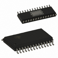
IC WIRELESS USB 2.4GHZ 28-SOIC
Manufacturer
Cypress Semiconductor Corp
Specifications of CYWUSB6934-28SEC
Frequency
2.4GHz
Data Rate - Maximum
62.5kbps
Modulation Or Protocol
DSSS, GFSK
Applications
HID, PC, Peripheral Gaming Devices
Power - Output
0dBm
Sensitivity
-90dBm
Voltage - Supply
2.7 V ~ 3.6 V
Data Interface
PCB, Surface Mount
Antenna Connector
PCB, Surface Mount
Operating Temperature
0°C ~ 70°C
Package / Case
28-SOIC
Operating Temperature (min)
0C
Operating Temperature (max)
70C
Operating Temperature Classification
Commercial
Operating Supply Voltage (min)
2.7V
Operating Supply Voltage (typ)
3V
Operating Supply Voltage (max)
3.6V
Lead Free Status / RoHS Status
Contains lead / RoHS non-compliant
Memory Size
-
Current - Transmitting
-
Current - Receiving
-
Lead Free Status / Rohs Status
Not Compliant
Other names
428-1580-5
Available stocks
Company
Part Number
Manufacturer
Quantity
Price
Company:

Part Number:
CYWUSB6934-28SEC
Manufacturer:
CY
Quantity:
22 751


Note:
Document 38-16007 Rev. *G
7.
Bit
7
6:0
Bit
7:6 Reserved
5
4:0 RSSI
Bit
7:3
2:0
Reserved
The RSSI will collect a single value each time the part is put into receive mode via Control register (Reg 0x03, bit 7=1). See Section 4.7 for more details.
Name
Valid
Name
Reserved
Channel
Name
Reserved
PA Bias
7
7
7
Addr: 0x21
Addr: 0x22
Addr: 0x23
Reserved
Description
This bit is reserved and should be written with zero.
The Channel register (Reg 0x21) is used to determine the Synthesizer frequency. A value of 2 corresponds to a communication
frequency of 2.402 GHz, while a value of 79 corresponds to a frequency of 2.479GHz. The channels are separated from each
other by 1 MHz intervals.
Limit application usage to channels 2-79 to adhere to FCC regulations. FCC regulations require that channels 0 and 1 and
any channel greater than 79 be avoided. Use of other channels may be restricted by other regulatory agencies. The application
MCU must ensure that this register is modified before transmitting data over the air for the first time.
Description
These bits are reserved. This register is read-only.
The Valid bit indicates whether the RSSI value in bits [4:0] are valid. This register is Read Only.
The Receive Strength Signal Indicator (RSSI) value indicates the strength of the received signal. This is a read only
value with the higher values indicating stronger received signals meaning more reliable transmissions.
Description
These bits are reserved and should be written with zeroes.
The Power Amplifier Bias (PA Bias) bits are used to set the transmit power of the IC through increasing (values up to 7) or
decreasing (values down to 0) the gain of the on-chip Power Amplifier. The higher the register value the higher the transmit
power. By changing the PA Bias value signal strength management functions can be accomplished. For general purpose
communication a value of 7 is recommended.
1 = RSSI value is valid
0 = RSSI value is invalid
6
6
6
Figure 7-23. Receive Signal Strength Indicator (RSSI)
Reserved
Valid
5
5
5
Figure 7-22. Channel
Figure 7-24. PA Bias
REG_CHANNEL
4
4
4
REG_RSSI
REG_PA
Channel
3
3
3
RSSI
2
2
2
[7]
PA Bias
1
1
1
CYWUSB6932
CYWUSB6934
Default: 0x00
Default: 0x00
Default: 0x00
Page 19 of 30
0
0
0
Related parts for CYWUSB6934-28SEC
Image
Part Number
Description
Manufacturer
Datasheet
Request
R

Part Number:
Description:
IC USB WIRELESS 2.4GHZ 48VQFN
Manufacturer:
Cypress Semiconductor Corp
Datasheet:
Part Number:
Description:
IC WIRELESS USB 2.4GHZ 48VQFN
Manufacturer:
Cypress Semiconductor Corp
Datasheet:

Part Number:
Description:
IC WIRELESS USB 2.4GHZ 48VQFN
Manufacturer:
Cypress Semiconductor Corp
Datasheet:
Part Number:
Description:
Manufacturer:
Cypress Semiconductor Corp
Datasheet:
Part Number:
Description:
Manufacturer:
Cypress Semiconductor Corp
Datasheet:
Part Number:
Description:
Manufacturer:
Cypress Semiconductor Corp
Datasheet:
Part Number:
Description:
Manufacturer:
Cypress Semiconductor Corp
Datasheet: