CYWUSB6934-28SEC Cypress Semiconductor Corp, CYWUSB6934-28SEC Datasheet - Page 2
CYWUSB6934-28SEC
Manufacturer Part Number
CYWUSB6934-28SEC
Description
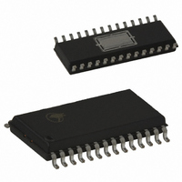
IC WIRELESS USB 2.4GHZ 28-SOIC
Manufacturer
Cypress Semiconductor Corp
Specifications of CYWUSB6934-28SEC
Frequency
2.4GHz
Data Rate - Maximum
62.5kbps
Modulation Or Protocol
DSSS, GFSK
Applications
HID, PC, Peripheral Gaming Devices
Power - Output
0dBm
Sensitivity
-90dBm
Voltage - Supply
2.7 V ~ 3.6 V
Data Interface
PCB, Surface Mount
Antenna Connector
PCB, Surface Mount
Operating Temperature
0°C ~ 70°C
Package / Case
28-SOIC
Operating Temperature (min)
0C
Operating Temperature (max)
70C
Operating Temperature Classification
Commercial
Operating Supply Voltage (min)
2.7V
Operating Supply Voltage (typ)
3V
Operating Supply Voltage (max)
3.6V
Lead Free Status / RoHS Status
Contains lead / RoHS non-compliant
Memory Size
-
Current - Transmitting
-
Current - Receiving
-
Lead Free Status / Rohs Status
Not Compliant
Other names
428-1580-5
Available stocks
Company
Part Number
Manufacturer
Quantity
Price
Company:

Part Number:
CYWUSB6934-28SEC
Manufacturer:
CY
Quantity:
22 751


3.1
The CYWUSB6932/CYWUSB6934 ICs are supported by the
CY3632 WirelessUSB Development Kit. The development kit
provides all of the materials and documents needed to cut the
cord on wired applications including two radio modules that
connect directly to two prototyping platform boards, compre-
hensive WirelessUSB protocol code examples a WirelessUSB
Listener tool and all of the associated schematics, gerber files
and bill of materials.
The CY4632 WirelessUSB LS Keyboard Mouse Reference
Design provides a production-worthy example of a wireless
mouse and keyboard system.
The CY3633 WirelessUSB LS Gaming Development Kit
provides support for designing a wireless gamepad for the
major gaming consoles and is offered as an accessory to the
CY3632 WirelessUSB.
4.0
The CYWUSB6932/CYWUSB6934 ICs provide a complete
WirelessUSB LS SPI to antenna radio modem. The SoC is
designed to implement wireless devices operating in the
worldwide 2.4-GHz Industrial, Scientific, and Medical (ISM)
frequency band (2.400 GHz–2.4835 GHz). It is intended for
systems compliant with world-wide regulations covered by
ETSI EN 301 489-1 V1.4.1, ETSI EN 300 328-1 V1.3.1
(European Countries); FCC CFR 47 Part 15 (USA and
Industry Canada) and ARIB STD-T66 (Japan).
The CYWUSB6934 IC contains a 2.4-GHz radio transceiver, a
GFSK modem and a dual DSSS reconfigurable baseband.
The CYWUSB6932 IC contains a 2.4-GHz radio transmit-only,
a GFSK modem and a DSSS baseband. The radio and
baseband are both code- and frequency-agile. Forty-nine
spreading codes selected for optimal performance (Gold
codes) are supported across 78 1-MHz channels yielding a
theoretical spectral capacity of 3822 channels. Both ICs
support a range of up to 10 meters or more.
4.1
The receiver and transmitter are a single-conversion low-Inter-
mediate Frequency (low-IF) architecture with fully integrated
IF channel matched filters to achieve high performance in the
presence of interference. An integrated Power Amplifier (PA)
provides an output power control range of 30 dB in seven
steps.
Table 4-1. Internal PA Output Power Step Table
Document 38-16007 Rev. *G
Applications Support
2.4-GHz Radio
PA Setting
Functional Overview
7
6
5
4
3
2
1
0
Typical Output Power (dBm)
–16.4
–20.8
–24.8
–29.0
–2.4
–5.6
–9.7
0
Both the receiver and transmitter integrated Voltage
Controlled Oscillator (VCO) and synthesizer have the agility to
cover the complete 2.4-GHz GFSK radio transmitter ISM
band. The synthesizer provides the frequency-hopping local
oscillator for the transmitter and receiver. The VCO loop filter
is also integrated on-chip.
4.2
The transmitter uses a DSP-based vector modulator to
convert the 1-MHz chips to an accurate GFSK carrier.
The receiver uses a fully integrated Frequency Modulator (FM)
detector with automatic data slicer to demodulate the GFSK
signal.
4.3
Data is converted to DSSS chips by a digital spreader.
De-spreading is performed by an oversampled correlator. The
DSSS baseband cancels spurious noise and assembles
properly correlated data bytes.
The DSSS baseband has three operating modes: 64 chips/bit
Single Channel, 32 chips/bit Single Channel, and 32 chips/bit
Single Channel Dual Data Rate (DDR).
4.3.1
The baseband supports a single data stream operating at
15.625 kbits/sec. The advantage of selecting this mode is its
ability to tolerate a noisy environment. This is because the
15.625 kbits/sec data stream utilizes the longest PN Code
resulting in the highest probability for recovering packets over
the air. This mode can also be selected for systems requiring
data transmissions over longer ranges.
4.3.2
The baseband supports a single data stream operating at
31.25 kbits/sec.
4.3.3
The baseband spreads bits in pairs and supports a single data
stream operating at 62.5 kbits/sec.
4.4
The CYWUSB6934 IC has a data Serializer/Deserializer
(SERDES), which provides byte-level framing of transmit and
receive data. Bytes for transmission are loaded into the
SERDES and receive bytes are read from the SERDES via the
SPI interface. The SERDES provides double buffering of
transmit and receive data. While one byte is being transmitted
by the radio the next byte can be written to the SERDES data
register insuring there are no breaks in transmitted data.
After a receive byte has been received it is loaded into the
SERDES data register and can be read at any time until the
next byte is received, at which time the old contents of the
SERDES data register will be overwritten. The CYWUSB6932
IC only has a data Serializer.
GFSK Modem
Dual DSSS Baseband
64 chips/bit Single Channel
32 chips/bit Single Channel
32 chips/bit Single Channel Dual Data Rate (DDR)
Serializer/Deserializer (SERDES)
CYWUSB6932
CYWUSB6934
Page 2 of 30
Related parts for CYWUSB6934-28SEC
Image
Part Number
Description
Manufacturer
Datasheet
Request
R

Part Number:
Description:
IC USB WIRELESS 2.4GHZ 48VQFN
Manufacturer:
Cypress Semiconductor Corp
Datasheet:
Part Number:
Description:
IC WIRELESS USB 2.4GHZ 48VQFN
Manufacturer:
Cypress Semiconductor Corp
Datasheet:

Part Number:
Description:
IC WIRELESS USB 2.4GHZ 48VQFN
Manufacturer:
Cypress Semiconductor Corp
Datasheet:
Part Number:
Description:
Manufacturer:
Cypress Semiconductor Corp
Datasheet:
Part Number:
Description:
Manufacturer:
Cypress Semiconductor Corp
Datasheet:
Part Number:
Description:
Manufacturer:
Cypress Semiconductor Corp
Datasheet:
Part Number:
Description:
Manufacturer:
Cypress Semiconductor Corp
Datasheet: