CYWUSB6934-28SEC Cypress Semiconductor Corp, CYWUSB6934-28SEC Datasheet - Page 20
CYWUSB6934-28SEC
Manufacturer Part Number
CYWUSB6934-28SEC
Description
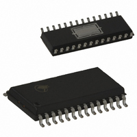
IC WIRELESS USB 2.4GHZ 28-SOIC
Manufacturer
Cypress Semiconductor Corp
Specifications of CYWUSB6934-28SEC
Frequency
2.4GHz
Data Rate - Maximum
62.5kbps
Modulation Or Protocol
DSSS, GFSK
Applications
HID, PC, Peripheral Gaming Devices
Power - Output
0dBm
Sensitivity
-90dBm
Voltage - Supply
2.7 V ~ 3.6 V
Data Interface
PCB, Surface Mount
Antenna Connector
PCB, Surface Mount
Operating Temperature
0°C ~ 70°C
Package / Case
28-SOIC
Operating Temperature (min)
0C
Operating Temperature (max)
70C
Operating Temperature Classification
Commercial
Operating Supply Voltage (min)
2.7V
Operating Supply Voltage (typ)
3V
Operating Supply Voltage (max)
3.6V
Lead Free Status / RoHS Status
Contains lead / RoHS non-compliant
Memory Size
-
Current - Transmitting
-
Current - Receiving
-
Lead Free Status / Rohs Status
Not Compliant
Other names
428-1580-5
Available stocks
Company
Part Number
Manufacturer
Quantity
Price
Company:

Part Number:
CYWUSB6934-28SEC
Manufacturer:
CY
Quantity:
22 751


Document 38-16007 Rev. *G
Bit
7
6
5:0
Bit
7:6
5:0
Bit
7
6:0
Reg Power
Reserved
Control
Name
Reserved
Clock Output
Disable
Crystal Adjust
Name
VCO Slope Enable
(Write-Only)
Reserved
Name
Reg Power
Control
Reserved
7
7
7
VCO Slope Enable
Addr: 0x2E
Addr: 0x24
Addr: 0x26
Clock Output
Description
When set, this bit disables unused circuitry and saves radio power. The user must set Reg 0x20, bit 6=1 to enable writes
to Reg 0x2E. The application MCU must set this bit during initialization.
These bits are reserved and should be written with zeroes.
Disable
6
6
6
Description
The Voltage Controlled Oscillator (VCO) Slope Enable bits are used to specify the amount of variance automatically
added to the VCO.
These bits are undefined for read operations.
These bits are reserved and should be written with zeroes.
Description
This bit is reserved and should be written with zero.
The Clock Output Disable bit disables the 13 MHz clock driven on the X13OUT pin.
If the 13 MHz clock is driven on the X13OUT pin then receive sensitivity will be reduced by -4 dBm on channels
5+13 n . By default the 13 MHz clock output pin is enabled. This pin is useful for adjusting the 13 MHz clock, but it
interfere with every 13th channel beginning with 2.405GHz channel. Therefore, it is recommended that the 13 MHz
clock output pin be disabled when not in use.
The Crystal Adjust value is used to calibrate the on-chip parallel load capacitance supplied to the crystal. Each
increment of the Crystal Adjust value typically adds 0.135 pF of parallel load capacitance. The total range is 8.5
pF, starting at 8.65 pF. These numbers do not include PCB parasitics, which can add an additional 1-2 pF.
11 = -5/+5 VCO adjust. The application MCU must configure this option during initialization.
10 = -2/+3 VCO adjust.
01 = Reserved.
00 = No VCO adjust.
1 = No 13 MHz clock driven externa
0 = 13 MHz clock driven externally
5
5
5
Figure 7-27. Reg Power Control
Figure 7-26. VCO Calibration
Figure 7-25. Crystal Adjust
REG_CRYSTAL_ADJ
4
REG_VCO_CAL
4
4
REG_PWR_CTL
.
ll
y
.
Reserved
3
3
3
Crystal Adjust
Reserved
2
2
2
1
1
1
CYWUSB6932
CYWUSB6934
Default: 0x00
Default: 0x00
Default: 0x00
Page 20 of 30
0
0
0
Related parts for CYWUSB6934-28SEC
Image
Part Number
Description
Manufacturer
Datasheet
Request
R

Part Number:
Description:
IC USB WIRELESS 2.4GHZ 48VQFN
Manufacturer:
Cypress Semiconductor Corp
Datasheet:
Part Number:
Description:
IC WIRELESS USB 2.4GHZ 48VQFN
Manufacturer:
Cypress Semiconductor Corp
Datasheet:

Part Number:
Description:
IC WIRELESS USB 2.4GHZ 48VQFN
Manufacturer:
Cypress Semiconductor Corp
Datasheet:
Part Number:
Description:
Manufacturer:
Cypress Semiconductor Corp
Datasheet:
Part Number:
Description:
Manufacturer:
Cypress Semiconductor Corp
Datasheet:
Part Number:
Description:
Manufacturer:
Cypress Semiconductor Corp
Datasheet:
Part Number:
Description:
Manufacturer:
Cypress Semiconductor Corp
Datasheet: