CYWUSB6934-28SEC Cypress Semiconductor Corp, CYWUSB6934-28SEC Datasheet - Page 22
CYWUSB6934-28SEC
Manufacturer Part Number
CYWUSB6934-28SEC
Description
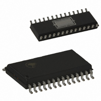
IC WIRELESS USB 2.4GHZ 28-SOIC
Manufacturer
Cypress Semiconductor Corp
Specifications of CYWUSB6934-28SEC
Frequency
2.4GHz
Data Rate - Maximum
62.5kbps
Modulation Or Protocol
DSSS, GFSK
Applications
HID, PC, Peripheral Gaming Devices
Power - Output
0dBm
Sensitivity
-90dBm
Voltage - Supply
2.7 V ~ 3.6 V
Data Interface
PCB, Surface Mount
Antenna Connector
PCB, Surface Mount
Operating Temperature
0°C ~ 70°C
Package / Case
28-SOIC
Operating Temperature (min)
0C
Operating Temperature (max)
70C
Operating Temperature Classification
Commercial
Operating Supply Voltage (min)
2.7V
Operating Supply Voltage (typ)
3V
Operating Supply Voltage (max)
3.6V
Lead Free Status / RoHS Status
Contains lead / RoHS non-compliant
Memory Size
-
Current - Transmitting
-
Current - Receiving
-
Lead Free Status / Rohs Status
Not Compliant
Other names
428-1580-5
Available stocks
Company
Part Number
Manufacturer
Quantity
Price
Company:

Part Number:
CYWUSB6934-28SEC
Manufacturer:
CY
Quantity:
22 751


8.0
Table 8-1. Pin Description Table for the CYWUSB6932/CYWUSB6934
Document 38-16007 Rev. *G
6, 9, 16, 28,
1, 2, 3, 4, 7,
29, 32, 41,
12, 15, 17,
18, 27, 30,
31, 36, 37,
39, 40, 43,
42, 44, 45
8, 10, 11,
Pin QFN
Exposed
Paddle
47, 48
46
38
35
26
33
14
34
20
19
21
23
24
25
22
13
5
Pin Definitions
RFIN
RFOUT
X13
X13IN
X13OUT
PD
RESET
PACTL
DIO
DIOVAL
IRQ
MOSI
MISO
SCK
SS
VCC
GND
NC
GND
Name
Output /Hi-Z
Output/Hi-Z
Output/Hi-Z
Output
Type
Input
Input
Input
Input
Input
Input
Input
Input
GND
GND
VCC
N/A
I/O
I/O
I/O
Default
Output System Clock . Buffered 13-MHz system clock.
Output IRQ . Interrupt and SERDES Bypass Mode DIOCLK.
Input
Input
Input
Input
Hi-Z
N/A
N/A
N/A
N/A
N/A
N/A
N/A
N/A
N/A
H
L
L
RF Input . Modulated RF signal received (CYWUSB6934 only).
RF Output . Modulated RF signal to be transmitted.
Crystal Input . (refer to Section 4.6 ).
Crystal Input . (refer to Section 4.6 ).
Power Down . Asserting this input (low), will put the
CYWUSB6932/CYWUSB6934 in the Suspend Mode (X13OUT is 0 when PD
is Low).
Active LOW Reset . Device reset.
PACTL . External Power Amplifier control. Pull-down or make output.
Data Input/Output. SERDES Bypass Mode Data Transmit/Receive.
Data I/O Valid . SERDES Bypass Mode Data Transmit/Receive Valid.
Master-Output-Slave-Input Data . SPI data input pin.
Master-Input-Slave-Output Data . SPI data output pin.
SPI Input Clock . SPI clock.
Slave Select Enable . SPI enable.
V
Ground = 0V .
Must be tied to Ground.
Must be tied to Ground.
CC
= 2.7V to 3.6V.
Description
CYWUSB6932
CYWUSB6934
Page 22 of 30
Related parts for CYWUSB6934-28SEC
Image
Part Number
Description
Manufacturer
Datasheet
Request
R

Part Number:
Description:
IC USB WIRELESS 2.4GHZ 48VQFN
Manufacturer:
Cypress Semiconductor Corp
Datasheet:
Part Number:
Description:
IC WIRELESS USB 2.4GHZ 48VQFN
Manufacturer:
Cypress Semiconductor Corp
Datasheet:

Part Number:
Description:
IC WIRELESS USB 2.4GHZ 48VQFN
Manufacturer:
Cypress Semiconductor Corp
Datasheet:
Part Number:
Description:
Manufacturer:
Cypress Semiconductor Corp
Datasheet:
Part Number:
Description:
Manufacturer:
Cypress Semiconductor Corp
Datasheet:
Part Number:
Description:
Manufacturer:
Cypress Semiconductor Corp
Datasheet:
Part Number:
Description:
Manufacturer:
Cypress Semiconductor Corp
Datasheet: