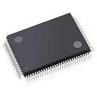
LCMXO256C-3TN100C Lattice, LCMXO256C-3TN100C Datasheet - Page 13

LCMXO256C-3TN100C
Manufacturer Part Number
LCMXO256C-3TN100C
Description
CPLD - Complex Programmable Logic Devices 256 LUTS 78 I/O
Manufacturer
Lattice
Series
MachXOr
Datasheet
1.LCMXO640C-3TN100C.pdf
(95 pages)
Specifications of LCMXO256C-3TN100C
Memory Type
SRAM
Number Of Macrocells
128
Delay Time
4.9 ns
Number Of Programmable I/os
78
Operating Supply Voltage
1.8 V, 2.5 V, 3.3 V
Supply Current
13 mA
Maximum Operating Temperature
+ 90 C
Minimum Operating Temperature
0 C
Package / Case
TQFP-100
Mounting Style
SMD/SMT
Supply Voltage (max)
3.465 V
Supply Voltage (min)
1.71 V
Cpld Type
FLASH
No. Of Macrocells
256
No. Of I/o's
78
Propagation Delay
4.9ns
Global Clock Setup Time
1.8ns
Frequency
420MHz
Supply Voltage Range
1.71V To 3.465V
Rohs Compliant
Yes
Programmable Type
In System Programmable
Delay Time Tpd(1) Max
4.9ns
Voltage Supply - Internal
1.71 V ~ 3.465 V
Number Of Logic Elements/blocks
-
Number Of Gates
-
Number Of I /o
78
Operating Temperature
0°C ~ 85°C
Mounting Type
*
Lead Free Status / RoHS Status
Lead free / RoHS Compliant
Available stocks
Company
Part Number
Manufacturer
Quantity
Price
Company:
Part Number:
LCMXO256C-3TN100C
Manufacturer:
LATTICE
Quantity:
5 600
Company:
Part Number:
LCMXO256C-3TN100C
Manufacturer:
LATTICE
Quantity:
5
Company:
Part Number:
LCMXO256C-3TN100C
Manufacturer:
LATTICE
Quantity:
35
Company:
Part Number:
LCMXO256C-3TN100C
Manufacturer:
Lattice Semiconductor Corporation
Quantity:
10 000
Part Number:
LCMXO256C-3TN100C
Manufacturer:
LATTICE
Quantity:
20 000
Lattice Semiconductor
Table 2-5. PLL Signal Descriptions
For more information on the PLL, please see details of additional technical documentation at the end of this data
sheet.
sysMEM Memory
The MachXO1200 and MachXO2280 devices contain sysMEM Embedded Block RAMs (EBRs). The EBR consists
of a 9-Kbit RAM, with dedicated input and output registers.
sysMEM Memory Block
The sysMEM block can implement single port, dual port, pseudo dual port, or FIFO memories. Each block can be
used in a variety of depths and widths as shown in Table 2-6.
Table 2-6. sysMEM Block Configurations
CLKI
CLKFB
RST
CLKOS
CLKOP
CLKOK
LOCK
CLKINTFB
DDAMODE
DDAIZR
DDAILAG
DDAIDEL[2:0]
Signal
I/O
O
O
O
O
O
I
I
I
I
I
I
I
Clock input from external pin or routing
PLL feedback input from PLL output, clock net, routing/external pin or internal feedback from
CLKINTFB port
“1” to reset the input clock divider
PLL output clock to clock tree (phase shifted/duty cycle changed)
PLL output clock to clock tree (No phase shift)
PLL output to clock tree through secondary clock divider
“1” indicates PLL LOCK to CLKI
Internal feedback source, CLKOP divider output before CLOCKTREE
Dynamic Delay Enable. “1”: Pin control (dynamic), “0”: Fuse Control (static)
Dynamic Delay Zero. “1”: delay = 0, “0”: delay = on
Dynamic Delay Lag/Lead. “1”: Lag, “0”: Lead
Dynamic Delay Input
Single Port
True Dual Port
Pseudo Dual Port
FIFO
Memory Mode
2-10
Configurations
8,192 x 1
4,096 x 2
2,048 x 4
1,024 x 9
256 x 36
8,192 x 1
4,096 x 2
2,048 x 4
1,024 x 9
512 x 18
8,192 x 1
4,096 x 2
2,048 x 4
1,024 x 9
512 x 18
256 x 36
8,192 x 1
4,096 x 2
2,048 x 4
1,024 x 9
512 x 18
256 x 36
512 x 18
Description
MachXO Family Data Sheet
Architecture


