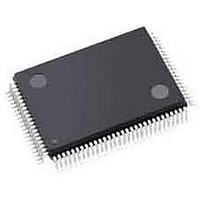
LCMXO256C-3TN100C Lattice, LCMXO256C-3TN100C Datasheet - Page 34

LCMXO256C-3TN100C
Manufacturer Part Number
LCMXO256C-3TN100C
Description
CPLD - Complex Programmable Logic Devices 256 LUTS 78 I/O
Manufacturer
Lattice
Series
MachXOr
Datasheet
1.LCMXO640C-3TN100C.pdf
(95 pages)
Specifications of LCMXO256C-3TN100C
Memory Type
SRAM
Number Of Macrocells
128
Delay Time
4.9 ns
Number Of Programmable I/os
78
Operating Supply Voltage
1.8 V, 2.5 V, 3.3 V
Supply Current
13 mA
Maximum Operating Temperature
+ 90 C
Minimum Operating Temperature
0 C
Package / Case
TQFP-100
Mounting Style
SMD/SMT
Supply Voltage (max)
3.465 V
Supply Voltage (min)
1.71 V
Cpld Type
FLASH
No. Of Macrocells
256
No. Of I/o's
78
Propagation Delay
4.9ns
Global Clock Setup Time
1.8ns
Frequency
420MHz
Supply Voltage Range
1.71V To 3.465V
Rohs Compliant
Yes
Programmable Type
In System Programmable
Delay Time Tpd(1) Max
4.9ns
Voltage Supply - Internal
1.71 V ~ 3.465 V
Number Of Logic Elements/blocks
-
Number Of Gates
-
Number Of I /o
78
Operating Temperature
0°C ~ 85°C
Mounting Type
*
Lead Free Status / RoHS Status
Lead free / RoHS Compliant
Available stocks
Company
Part Number
Manufacturer
Quantity
Price
Company:
Part Number:
LCMXO256C-3TN100C
Manufacturer:
LATTICE
Quantity:
5 600
Company:
Part Number:
LCMXO256C-3TN100C
Manufacturer:
LATTICE
Quantity:
5
Company:
Part Number:
LCMXO256C-3TN100C
Manufacturer:
LATTICE
Quantity:
35
Company:
Part Number:
LCMXO256C-3TN100C
Manufacturer:
Lattice Semiconductor Corporation
Quantity:
10 000
Part Number:
LCMXO256C-3TN100C
Manufacturer:
LATTICE
Quantity:
20 000
Lattice Semiconductor
sysIO Differential Electrical Characteristics
LVDS
LVDS Emulation
MachXO devices can support LVDS outputs via emulation (LVDS25E), in addition to the LVDS support that is avail-
able on-chip on certain devices. The output is emulated using complementary LVCMOS outputs in conjunction with
resistors across the driver outputs on all devices. The scheme shown in Figure 3-1 is one possible solution for
LVDS standard implementation. Resistor values in Figure 3-1 are industry standard values for 1% resistors.
Figure 3-1. LVDS Using External Resistors (LVDS25E)
The LVDS differential input buffers are available on certain devices in the MachXO family.
V
V
V
I
V
V
V
ΔV
V
ΔV
I
IN
OSD
Parameter
OH
OL
OD
OS
INP,
THD
CM
Symbol
OD
OS
V
INM
Input Voltage
Differential Input Threshold
Input Common Mode Voltage
Input current
Output high voltage for V
Output low voltage for V
Output voltage differential
Change in V
low
Output voltage offset
Change in V
Output short circuit current
Parameter Description
8mA
8mA
Note: All resistors are ±1%.
OD
OS
VCCIO = 2.5
VCCIO = 2.5
between H and L
between high and
Emulated
On-chip
Buffer
LVDS
Over Recommended Operating Conditions
OP
OP
or V
or V
OM
OM
Off-chip
158
158
100mV ≤ V
200mV ≤ V
350mV ≤ V
Power on
R
R
(V
(V
V
shorted
OD
T
T
OP
OP
= 100 Ohm
= 100 Ohm
= 0V Driver outputs
- V
- V
Test Conditions
140
OM
OM
3-8
THD
THD
THD
), R
)/2, R
T
= 100 Ohm
T
Zo = 100
= 100 Ohm
DC and Switching Characteristics
V
V
V
Off-chip
+/-100
1.125
Min.
0.9V
THD
THD
THD
250
—
—
—
—
—
MachXO Family Data Sheet
0
100
/2
/2
/2
Typ.
1.38
1.03
1.25
350
1.2
1.2
1.2
—
—
—
—
—
—
On-chip
+
-
1.375
+/-10
Max.
1.60
450
2.4
1.8
1.9
2.0
50
50
—
—
6
Units
mV
mV
mV
mV
mA
µA
V
V
V
V
V
V
V


