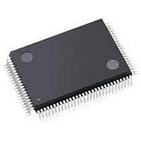
LCMXO256C-3TN100C Lattice, LCMXO256C-3TN100C Datasheet - Page 21

LCMXO256C-3TN100C
Manufacturer Part Number
LCMXO256C-3TN100C
Description
CPLD - Complex Programmable Logic Devices 256 LUTS 78 I/O
Manufacturer
Lattice
Series
MachXOr
Datasheet
1.LCMXO640C-3TN100C.pdf
(95 pages)
Specifications of LCMXO256C-3TN100C
Memory Type
SRAM
Number Of Macrocells
128
Delay Time
4.9 ns
Number Of Programmable I/os
78
Operating Supply Voltage
1.8 V, 2.5 V, 3.3 V
Supply Current
13 mA
Maximum Operating Temperature
+ 90 C
Minimum Operating Temperature
0 C
Package / Case
TQFP-100
Mounting Style
SMD/SMT
Supply Voltage (max)
3.465 V
Supply Voltage (min)
1.71 V
Cpld Type
FLASH
No. Of Macrocells
256
No. Of I/o's
78
Propagation Delay
4.9ns
Global Clock Setup Time
1.8ns
Frequency
420MHz
Supply Voltage Range
1.71V To 3.465V
Rohs Compliant
Yes
Programmable Type
In System Programmable
Delay Time Tpd(1) Max
4.9ns
Voltage Supply - Internal
1.71 V ~ 3.465 V
Number Of Logic Elements/blocks
-
Number Of Gates
-
Number Of I /o
78
Operating Temperature
0°C ~ 85°C
Mounting Type
*
Lead Free Status / RoHS Status
Lead free / RoHS Compliant
Available stocks
Company
Part Number
Manufacturer
Quantity
Price
Company:
Part Number:
LCMXO256C-3TN100C
Manufacturer:
LATTICE
Quantity:
5 600
Company:
Part Number:
LCMXO256C-3TN100C
Manufacturer:
LATTICE
Quantity:
5
Company:
Part Number:
LCMXO256C-3TN100C
Manufacturer:
LATTICE
Quantity:
35
Company:
Part Number:
LCMXO256C-3TN100C
Manufacturer:
Lattice Semiconductor Corporation
Quantity:
10 000
Part Number:
LCMXO256C-3TN100C
Manufacturer:
LATTICE
Quantity:
20 000
Lattice Semiconductor
Table 2-10. Supported Output Standards
sysIO Buffer Banks
The number of Banks vary between the devices of this family. Eight Banks surround the two larger devices, the
MachXO1200 and MachXO2280 (two Banks per side). The MachXO640 has four Banks (one Bank per side). The
smallest member of this family, the MachXO256, has only two Banks.
Each sysIO buffer Bank is capable of supporting multiple I/O standards. Each Bank has its own I/O supply voltage
(V
and Figure 2-21 shows the sysIO Banks and their associated supplies for all devices.
CCIO
) which allows it to be completely independent from the other Banks. Figure 2-18, Figure 2-18, Figure 2-20
Single-ended Interfaces
LVTTL
LVCMOS33
LVCMOS25
LVCMOS18
LVCMOS15
LVCMOS12
LVCMOS33, Open Drain
LVCMOS25, Open Drain
LVCMOS18, Open Drain
LVCMOS15, Open Drain
LVCMOS12, Open Drain
PCI33
Differential Interfaces
LVDS
BLVDS, RSDS
LVPECL
1. MachXO1200 and MachXO2280 devices have dedicated LVDS buffers.
2. These interfaces can be emulated with external resistors in all devices.
3. Top Banks of MachXO1200 and MachXO2280 devices only.
1, 2
3
2
Output Standard
2
2-18
4mA, 8mA, 12mA, 16mA
4mA, 8mA, 12mA, 14mA
4mA, 8mA, 12mA, 14mA
4mA, 8mA, 12mA, 14mA
4mA, 8mA, 12mA, 14mA
4mA, 8mA, 12mA, 14mA
4mA, 8mA, 12mA, 14mA
4mA, 8mA
2mA, 6mA
4mA, 8mA
2mA, 6mA
Drive
N/A
N/A
N/A
N/A
MachXO Family Data Sheet
V
CCIO
3.3
3.3
2.5
1.8
1.5
1.2
3.3
2.5
2.5
3.3
—
—
—
—
—
(Typ.)
Architecture


