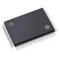
LCMXO256C-3TN100C Lattice, LCMXO256C-3TN100C Datasheet - Page 37

LCMXO256C-3TN100C
Manufacturer Part Number
LCMXO256C-3TN100C
Description
CPLD - Complex Programmable Logic Devices 256 LUTS 78 I/O
Manufacturer
Lattice
Series
MachXOr
Datasheet
1.LCMXO640C-3TN100C.pdf
(95 pages)
Specifications of LCMXO256C-3TN100C
Memory Type
SRAM
Number Of Macrocells
128
Delay Time
4.9 ns
Number Of Programmable I/os
78
Operating Supply Voltage
1.8 V, 2.5 V, 3.3 V
Supply Current
13 mA
Maximum Operating Temperature
+ 90 C
Minimum Operating Temperature
0 C
Package / Case
TQFP-100
Mounting Style
SMD/SMT
Supply Voltage (max)
3.465 V
Supply Voltage (min)
1.71 V
Cpld Type
FLASH
No. Of Macrocells
256
No. Of I/o's
78
Propagation Delay
4.9ns
Global Clock Setup Time
1.8ns
Frequency
420MHz
Supply Voltage Range
1.71V To 3.465V
Rohs Compliant
Yes
Programmable Type
In System Programmable
Delay Time Tpd(1) Max
4.9ns
Voltage Supply - Internal
1.71 V ~ 3.465 V
Number Of Logic Elements/blocks
-
Number Of Gates
-
Number Of I /o
78
Operating Temperature
0°C ~ 85°C
Mounting Type
*
Lead Free Status / RoHS Status
Lead free / RoHS Compliant
Available stocks
Company
Part Number
Manufacturer
Quantity
Price
Company:
Part Number:
LCMXO256C-3TN100C
Manufacturer:
LATTICE
Quantity:
5 600
Company:
Part Number:
LCMXO256C-3TN100C
Manufacturer:
LATTICE
Quantity:
5
Company:
Part Number:
LCMXO256C-3TN100C
Manufacturer:
LATTICE
Quantity:
35
Company:
Part Number:
LCMXO256C-3TN100C
Manufacturer:
Lattice Semiconductor Corporation
Quantity:
10 000
Part Number:
LCMXO256C-3TN100C
Manufacturer:
LATTICE
Quantity:
20 000
Lattice Semiconductor
For further information on LVPECL, BLVDS and other differential interfaces please see details of additional techni-
cal documentation at the end of the data sheet.
RSDS
The MachXO family supports the differential RSDS standard. The output standard is emulated using complemen-
tary LVCMOS outputs in conjunction with a parallel resistor across the driver outputs on all the devices. The RSDS
input standard is supported by the LVDS differential input buffer on certain devices. The scheme shown in Figure 3-
4 is one possible solution for RSDS standard implementation. Use LVDS25E mode with suggested resistors for
RSDS operation. Resistor values in Figure 3-4 are industry standard values for 1% resistors.
Figure 3-4. RSDS (Reduced Swing Differential Standard)
Table 3-4. RSDS DC Conditions
VCCIO = 2.5V
8mA
8mA
VCCIO = 2.5V
RSDS Buffer
Emulated
Z
R
R
R
V
V
V
V
Z
I
On-chip
DC
OUT
OH
OL
OD
BACK
S
P
T
CM
Parameter
Off-chip
Output impedance
Driver series resistor
Driver parallel resistor
Receiver termination
Output high voltage
Output low voltage
Output differential voltage
Output common mode voltage
Back impedance
DC output current
294
294
Description
121
3-11
Zo = 100
DC and Switching Characteristics
Typical
101.5
1.35
1.15
0.20
1.25
3.66
294
121
100
20
Off-chip
MachXO Family Data Sheet
Units
100
ohm
ohm
ohm
ohm
ohm
mA
V
V
V
V
On-chip
+
-


