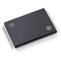
LCMXO256C-3TN100C Lattice, LCMXO256C-3TN100C Datasheet - Page 44

LCMXO256C-3TN100C
Manufacturer Part Number
LCMXO256C-3TN100C
Description
CPLD - Complex Programmable Logic Devices 256 LUTS 78 I/O
Manufacturer
Lattice
Series
MachXOr
Datasheet
1.LCMXO640C-3TN100C.pdf
(95 pages)
Specifications of LCMXO256C-3TN100C
Memory Type
SRAM
Number Of Macrocells
128
Delay Time
4.9 ns
Number Of Programmable I/os
78
Operating Supply Voltage
1.8 V, 2.5 V, 3.3 V
Supply Current
13 mA
Maximum Operating Temperature
+ 90 C
Minimum Operating Temperature
0 C
Package / Case
TQFP-100
Mounting Style
SMD/SMT
Supply Voltage (max)
3.465 V
Supply Voltage (min)
1.71 V
Cpld Type
FLASH
No. Of Macrocells
256
No. Of I/o's
78
Propagation Delay
4.9ns
Global Clock Setup Time
1.8ns
Frequency
420MHz
Supply Voltage Range
1.71V To 3.465V
Rohs Compliant
Yes
Programmable Type
In System Programmable
Delay Time Tpd(1) Max
4.9ns
Voltage Supply - Internal
1.71 V ~ 3.465 V
Number Of Logic Elements/blocks
-
Number Of Gates
-
Number Of I /o
78
Operating Temperature
0°C ~ 85°C
Mounting Type
*
Lead Free Status / RoHS Status
Lead free / RoHS Compliant
Available stocks
Company
Part Number
Manufacturer
Quantity
Price
Company:
Part Number:
LCMXO256C-3TN100C
Manufacturer:
LATTICE
Quantity:
5 600
Company:
Part Number:
LCMXO256C-3TN100C
Manufacturer:
LATTICE
Quantity:
5
Company:
Part Number:
LCMXO256C-3TN100C
Manufacturer:
LATTICE
Quantity:
35
Company:
Part Number:
LCMXO256C-3TN100C
Manufacturer:
Lattice Semiconductor Corporation
Quantity:
10 000
Part Number:
LCMXO256C-3TN100C
Manufacturer:
LATTICE
Quantity:
20 000
Lattice Semiconductor
Switching Test Conditions
Figure 3-5 shows the output test load that is used for AC testing. The specific values for resistance, capacitance,
voltage, and other test conditions are shown in Figure 3-5.
Figure 3-5. Output Test Load, LVTTL and LVCMOS Standards
Table 3-5. Test Fixture Required Components, Non-Terminated Interfaces
LVTTL and LVCMOS settings (L -> H, H -> L)
LVTTL and LVCMOS 3.3 (Z -> H)
LVTTL and LVCMOS 3.3 (Z -> L)
Other LVCMOS (Z -> H)
Other LVCMOS (Z -> L)
LVTTL + LVCMOS (H -> Z)
LVTTL + LVCMOS (L -> Z)
Note: Output test conditions for all other interfaces are determined by the respective standards.
Test Condition
DUT
V
R1
T
3-18
188
R
∞
1
CL
0pF
0pF
C
L
Test Poi nt
DC and Switching Characteristics
LVTTL, LVCMOS 3.3 = 1.5V
LVCMOS 2.5 = V
LVCMOS 1.8 = V
LVCMOS 1.5 = V
LVCMOS 1.2 = V
1.5
V
V
V
V
OH
OL
CCIO
CCIO
- 0.15
- 0.15
/2
/2
MachXO Family Data Sheet
Timing Ref.
CCIO
CCIO
CCIO
CCIO
/2
/2
/2
/2
V
V
V
V
V
V
V
—
—
—
—
—
OH
OH
OH
OL
OL
OL
T


