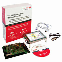
YLCDRSK2378 Renesas Electronics America, YLCDRSK2378 Datasheet - Page 1090

YLCDRSK2378
Manufacturer Part Number
YLCDRSK2378
Description
KIT DEV EVAL H8S/2378 LCD
Manufacturer
Renesas Electronics America
Series
H8®r
Datasheet
1.YR0K42378FC000BA.pdf
(1208 pages)
Specifications of YLCDRSK2378
Main Purpose
Displays, LCD Controller
Embedded
Yes, MCU, 16-Bit
Utilized Ic / Part
YLCDRSK2378
Primary Attributes
5.7" QVGA, Touch Screen
Secondary Attributes
Source Code on CD, Debugging Requires Emulator Cable E10A USB/JTAG
Lead Free Status / RoHS Status
Lead free / RoHS Compliant
- Current page: 1090 of 1208
- Download datasheet (8Mb)
Section 26 Electrical Characteristics
Notes: 1. When the A/D and D/A converters are not used, the AV
Table 26.4 Permissible Output Currents
Conditions: V
Item
Permissible output low
current (per pin)
Permissible output low
current (total)
Permissible output high
current (per pin)
Permissible output high
current (total)
Caution:
Note:
Rev.7.00 Mar. 18, 2009 page 1022 of 1136
REJ09B0109-0700
Item
Reference
power
supply
current
RAM standby voltage
2. Current consumption values are for V
3. The values are for V
4. I
* When the A/D and D/A converters are not used, do not leave the AV
I
I
not be open. Connect the AV
output pins unloaded and all input pull-up MOSs in the off state.
To protect the LSI’s reliability, do not exceed the output current values in table 26.4.
pins should not be open. Connect the AV
to V
CC
CC
CC
V
T
During A/D and
D/A conversion
Idle
max = 1.0 (mA) + 1.0 (mA/(MHz × V)) × V
max = 1.0 (mA) + 0.85 (mA/(MHz × V)) × V
depends on V
a
CC
SS
SS
= −40°C to +85°C (wide-range specifications)
.
= AV
= 3.0 V to 3.6 V, AV
SS
= 0 V * , T
Total of all output
pins
All output pins
Total of all output
pins
SCL0, 1, SDA0, 1
Output pins other
than the above
CC
and f as follows:
RAM
Symbol
AI
V
RAM
CC
a
≤ V
= −20°C to +75°C (regular specifications),
CC
CC
CC
< 3.0 V, V
= 3.0 V to 3.6 V, V
and V
Min.
⎯
⎯
2.0
Symbol
ΣI
−I
Σ−I
I
OL
IH
ref
OH
OL
min = V
OH
pins to V
IH
CC
min = V
CC
and V
CC
Typ.
3.0
(3.0 V)
0.01
⎯
CC
× f (normal operation)
× f (sleep mode)
Min.
⎯
⎯
⎯
⎯
⎯
CC
−0.2 V and V
CC
ref
ref
, and the AV
pins to V
× 0.9, and V
= 3.0 V to AV
Max.
6.0
5.0
⎯
CC
, V
Typ.
⎯
⎯
⎯
⎯
⎯
ref
CC
, and AV
IL
, and the AV
SS
max = 0.2 V with all
IL
max = 0.3 V.
pin to V
Unit
mA
μA
V
CC
CC
Max.
80
2.0
40
8.0
2.0
,
, V
SS
Test
Conditions
ref
pins should
SS
, and AV
SS
.
pin
Unit
mA
mA
mA
mA
SS
Related parts for YLCDRSK2378
Image
Part Number
Description
Manufacturer
Datasheet
Request
R

Part Number:
Description:
KIT STARTER FOR M16C/29
Manufacturer:
Renesas Electronics America
Datasheet:

Part Number:
Description:
KIT STARTER FOR R8C/2D
Manufacturer:
Renesas Electronics America
Datasheet:

Part Number:
Description:
R0K33062P STARTER KIT
Manufacturer:
Renesas Electronics America
Datasheet:

Part Number:
Description:
KIT STARTER FOR R8C/23 E8A
Manufacturer:
Renesas Electronics America
Datasheet:

Part Number:
Description:
KIT STARTER FOR R8C/25
Manufacturer:
Renesas Electronics America
Datasheet:

Part Number:
Description:
KIT STARTER H8S2456 SHARPE DSPLY
Manufacturer:
Renesas Electronics America
Datasheet:

Part Number:
Description:
KIT STARTER FOR R8C38C
Manufacturer:
Renesas Electronics America
Datasheet:

Part Number:
Description:
KIT STARTER FOR R8C35C
Manufacturer:
Renesas Electronics America
Datasheet:

Part Number:
Description:
KIT STARTER FOR R8CL3AC+LCD APPS
Manufacturer:
Renesas Electronics America
Datasheet:

Part Number:
Description:
KIT STARTER FOR RX610
Manufacturer:
Renesas Electronics America
Datasheet:

Part Number:
Description:
KIT STARTER FOR R32C/118
Manufacturer:
Renesas Electronics America
Datasheet:

Part Number:
Description:
KIT DEV RSK-R8C/26-29
Manufacturer:
Renesas Electronics America
Datasheet:

Part Number:
Description:
KIT STARTER FOR SH7124
Manufacturer:
Renesas Electronics America
Datasheet:

Part Number:
Description:
KIT STARTER FOR H8SX/1622
Manufacturer:
Renesas Electronics America
Datasheet:

Part Number:
Description:
KIT DEV FOR SH7203
Manufacturer:
Renesas Electronics America
Datasheet:


