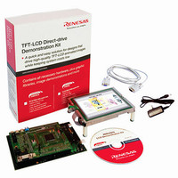
YLCDRSK2378 Renesas Electronics America, YLCDRSK2378 Datasheet - Page 520

YLCDRSK2378
Manufacturer Part Number
YLCDRSK2378
Description
KIT DEV EVAL H8S/2378 LCD
Manufacturer
Renesas Electronics America
Series
H8®r
Datasheet
1.YR0K42378FC000BA.pdf
(1208 pages)
Specifications of YLCDRSK2378
Main Purpose
Displays, LCD Controller
Embedded
Yes, MCU, 16-Bit
Utilized Ic / Part
YLCDRSK2378
Primary Attributes
5.7" QVGA, Touch Screen
Secondary Attributes
Source Code on CD, Debugging Requires Emulator Cable E10A USB/JTAG
Lead Free Status / RoHS Status
Lead free / RoHS Compliant
- Current page: 520 of 1208
- Download datasheet (8Mb)
Section 9 Data Transfer Controller (DTC)
9.7.4
An example is shown in which the DTC is used to transfer a block of 128 bytes of data by means
of software activation. The transfer source address is H'1000 and the destination address is
H'2000. The vector number is H'60, so the vector address is H'04C0.
1. Set MRA to incrementing source address (SM1 = 1, SM0 = 0), incrementing destination
2. Set the start address of the register information at the DTC vector address (H'04C0).
3. Check that the SWDTE bit in DTVECR is 0. Check that there is currently no transfer activated
4. Write 1 to the SWDTE bit and the vector number (H'60) to DTVECR. The write data is H'E0.
5. Read DTVECR again and check that it is set to the vector number (H'60). If it is not, this
6. If the write was successful, the DTC is activated and a block of 128 bytes of data is transferred.
7. After the transfer, an SWDTEND interrupt occurs. The interrupt handling routine should clear
9.8
9.8.1
DTC operation can be disabled or enabled using the module stop control register. The initial
setting is for DTC operation to be enabled. Register access is disabled by setting module stop
mode. Module stop mode cannot be set while the DTC is activated. For details, refer to section 24,
Power-Down Modes.
9.8.2
The MRA, MRB, SAR, DAR, CRA, and CRB registers are all located in on-chip RAM. When the
DTC is used, the RAME bit in SYSCR must not be cleared to 0.
Rev.7.00 Mar. 18, 2009 page 452 of 1136
REJ09B0109-0700
address (DM1 = 1, DM0 = 0), block transfer mode (MD1 = 1, MD0 = 0), and byte size (Sz =
0). The DTS bit can have any value. Set MRB for one block transfer by one interrupt (CHNE =
0). Set the transfer source address (H'1000) in SAR, the destination address (H'2000) in DAR,
and 128 (H'8080) in CRA. Set 1 (H'0001) in CRB.
by software.
indicates that the write failed. This is presumably because an interrupt occurred between steps
3 and 4 and led to a different software activation. To activate this transfer, go back to step 3.
the SWDTE bit to 0 and perform other wrap-up processing.
Software Activation
Usage Notes
Module Stop Mode Setting
On-Chip RAM
Related parts for YLCDRSK2378
Image
Part Number
Description
Manufacturer
Datasheet
Request
R

Part Number:
Description:
KIT STARTER FOR M16C/29
Manufacturer:
Renesas Electronics America
Datasheet:

Part Number:
Description:
KIT STARTER FOR R8C/2D
Manufacturer:
Renesas Electronics America
Datasheet:

Part Number:
Description:
R0K33062P STARTER KIT
Manufacturer:
Renesas Electronics America
Datasheet:

Part Number:
Description:
KIT STARTER FOR R8C/23 E8A
Manufacturer:
Renesas Electronics America
Datasheet:

Part Number:
Description:
KIT STARTER FOR R8C/25
Manufacturer:
Renesas Electronics America
Datasheet:

Part Number:
Description:
KIT STARTER H8S2456 SHARPE DSPLY
Manufacturer:
Renesas Electronics America
Datasheet:

Part Number:
Description:
KIT STARTER FOR R8C38C
Manufacturer:
Renesas Electronics America
Datasheet:

Part Number:
Description:
KIT STARTER FOR R8C35C
Manufacturer:
Renesas Electronics America
Datasheet:

Part Number:
Description:
KIT STARTER FOR R8CL3AC+LCD APPS
Manufacturer:
Renesas Electronics America
Datasheet:

Part Number:
Description:
KIT STARTER FOR RX610
Manufacturer:
Renesas Electronics America
Datasheet:

Part Number:
Description:
KIT STARTER FOR R32C/118
Manufacturer:
Renesas Electronics America
Datasheet:

Part Number:
Description:
KIT DEV RSK-R8C/26-29
Manufacturer:
Renesas Electronics America
Datasheet:

Part Number:
Description:
KIT STARTER FOR SH7124
Manufacturer:
Renesas Electronics America
Datasheet:

Part Number:
Description:
KIT STARTER FOR H8SX/1622
Manufacturer:
Renesas Electronics America
Datasheet:

Part Number:
Description:
KIT DEV FOR SH7203
Manufacturer:
Renesas Electronics America
Datasheet:


