YLCDRSK2378 Renesas Electronics America, YLCDRSK2378 Datasheet - Page 443
YLCDRSK2378
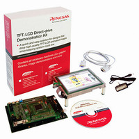
Manufacturer Part Number
YLCDRSK2378
Description
KIT DEV EVAL H8S/2378 LCD
Manufacturer
Renesas Electronics America
Series
H8®r
Datasheet
1.YR0K42378FC000BA.pdf
(1208 pages)
Specifications of YLCDRSK2378
Main Purpose
Displays, LCD Controller
Embedded
Yes, MCU, 16-Bit
Utilized Ic / Part
YLCDRSK2378
Primary Attributes
5.7" QVGA, Touch Screen
Secondary Attributes
Source Code on CD, Debugging Requires Emulator Cable E10A USB/JTAG
Lead Free Status / RoHS Status
Lead free / RoHS Compliant


Section 8 EXDMA Controller (EXDMAC)
In block transfer mode, a transfer of the specified block size is executed in response to one transfer
request. The block size can be from 1 to 256 bytes or words. Within a block, transfer can be
performed at the same high speed as in block transfer mode.
When the “no specification” setting (EDTCR = H'000000) is made for the number of transfers, the
transfer counter is halted and there is no limit on the number of transfers, allowing transfer to be
performed endlessly.
Incrementing or decrementing the memory address by 1 or 2, or leaving the address unchanged,
can be specified independently for each address register.
In all transfer modes, it is possible to set a repeat area comprising a power-of-two number of
bytes.
8.4.2
Address Modes
Dual Address Mode: In dual address mode, both the transfer source and transfer destination are
specified by registers in the EXDMAC, and one transfer is executed in two bus cycles.
The transfer source address is set in the source address register (EDSAR), and the transfer
destination address is set in the transfer destination address register (EDDAR).
In a transfer operation, the value in external memory specified by the transfer source address is
read in the first bus cycle, and is written to the external memory specified by the transfer
destination address in the next bus cycle.
These consecutive read and write cycles are indivisible: another bus cycle (external access by an
internal bus master, refresh cycle, or external bus release cycle) does not occur between these two
cycles.
ETEND pin output can be enabled or disabled by means of the ETENDE bit in EDMDR. ETEND
is output for two consecutive bus cycles. The EDACK signal is not output.
Figure 8.2 shows an example of the timing in dual address mode.
Rev.7.00 Mar. 18, 2009 page 375 of 1136
REJ09B0109-0700
Related parts for YLCDRSK2378
Image
Part Number
Description
Manufacturer
Datasheet
Request
R

Part Number:
Description:
KIT STARTER FOR M16C/29
Manufacturer:
Renesas Electronics America
Datasheet:

Part Number:
Description:
KIT STARTER FOR R8C/2D
Manufacturer:
Renesas Electronics America
Datasheet:

Part Number:
Description:
R0K33062P STARTER KIT
Manufacturer:
Renesas Electronics America
Datasheet:

Part Number:
Description:
KIT STARTER FOR R8C/23 E8A
Manufacturer:
Renesas Electronics America
Datasheet:

Part Number:
Description:
KIT STARTER FOR R8C/25
Manufacturer:
Renesas Electronics America
Datasheet:

Part Number:
Description:
KIT STARTER H8S2456 SHARPE DSPLY
Manufacturer:
Renesas Electronics America
Datasheet:

Part Number:
Description:
KIT STARTER FOR R8C38C
Manufacturer:
Renesas Electronics America
Datasheet:

Part Number:
Description:
KIT STARTER FOR R8C35C
Manufacturer:
Renesas Electronics America
Datasheet:

Part Number:
Description:
KIT STARTER FOR R8CL3AC+LCD APPS
Manufacturer:
Renesas Electronics America
Datasheet:
Part Number:
Description:
KIT STARTER FOR RX610
Manufacturer:
Renesas Electronics America
Datasheet:

Part Number:
Description:
KIT STARTER FOR R32C/118
Manufacturer:
Renesas Electronics America
Datasheet:

Part Number:
Description:
KIT DEV RSK-R8C/26-29
Manufacturer:
Renesas Electronics America
Datasheet:

Part Number:
Description:
KIT STARTER FOR SH7124
Manufacturer:
Renesas Electronics America
Datasheet:

Part Number:
Description:
KIT STARTER FOR H8SX/1622
Manufacturer:
Renesas Electronics America
Datasheet:

Part Number:
Description:
KIT DEV FOR SH7203
Manufacturer:
Renesas Electronics America
Datasheet: