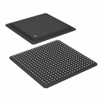
ADSP-21160MKBZ-80 Analog Devices Inc, ADSP-21160MKBZ-80 Datasheet - Page 34

ADSP-21160MKBZ-80
Manufacturer Part Number
ADSP-21160MKBZ-80
Description
32bit SHARC W/SIMD Capability
Manufacturer
Analog Devices Inc
Series
SHARC®r
Type
Floating Pointr
Specifications of ADSP-21160MKBZ-80
Interface
Host Interface, Link Port, Serial Port
Clock Rate
80MHz
Non-volatile Memory
External
On-chip Ram
512kB
Voltage - I/o
3.30V
Voltage - Core
2.50V
Operating Temperature
0°C ~ 85°C
Mounting Type
Surface Mount
Package / Case
400-BGA
Device Core Size
32b
Architecture
Enhanced Harvard
Format
Floating Point
Clock Freq (max)
80MHz
Mips
80
Device Input Clock Speed
80MHz
Ram Size
512KB
Operating Supply Voltage (typ)
2.5/3.3V
Operating Supply Voltage (min)
2.37/3.13V
Operating Supply Voltage (max)
2.63/3.47V
Operating Temp Range
0C to 85C
Operating Temperature Classification
Commercial
Mounting
Surface Mount
Pin Count
400
Package Type
BGA
Lead Free Status / RoHS Status
Lead free / RoHS Compliant
Lead Free Status / RoHS Status
Lead free / RoHS Compliant, Lead free / RoHS Compliant
Available stocks
Company
Part Number
Manufacturer
Quantity
Price
Company:
Part Number:
ADSP-21160MKBZ-80
Manufacturer:
AD
Quantity:
310
Company:
Part Number:
ADSP-21160MKBZ-80
Manufacturer:
Analog Devices Inc
Quantity:
10 000
ADSP-21160M
Link Ports
Calculation of link receiver data setup and hold relative to
link clock is required to determine the maximum allowable
skew that can be introduced in the transmission path
between LDATA and LCLK. Setup skew is the maximum
delay that can be introduced in LDATA relative to LCLK
(setup skew = t
maximum delay that can be introduced in LCLK relative to
LDATA (hold skew = t
lations made directly from speed specifications will result in
unrealistically small skew times because they include
multiple tester guardbands.
Note that there is a two-cycle effect latency between the link
port enable instruction and the DSP enabling the link port.
Maximum throughput varies across link port trans-
mit/receive pairs.
all transmit/receive pairs based on setup skew of 0.5 ns
(setup skew=t
results indicate 80 MHz operation across all link ports. All
hold time skews are equal to 0.5 ns or greater for all link
port transmit/receive pairs at 80 MHz. Based upon these
values, all link port transmit/receive pairs can be operated
at maximum throughput for LxCLK:CCLK ratios of 2:1,
3:1, and 4:1 at 80 MHz CCLK. To operate all link port
transmit/receive pairs at LxCLK:CCLK ratio of 1:1, the
core clock frequency must be no greater than 62.5 MHz.
Maximum data throughput values are based upon the reset
value of the LAR Link Port Assignment Register (Link
Buffer 0 assigned to Link Port 0, Link Buffer 1 assigned to
Link Port 1, etc.). Throughputs are not guaranteed for LAR
settings other than the reset LAR value. For additional
details on LAR, refer to the ADSP-21160 DSP Hardware
Reference manual.
Table 18. Link Port—Maximum Data Throughput for
Transmit/Receive Pairs
Transmit
Link Port
0
1
LCLKTWH
LCLKTWH
Receive
Link Port
0
1
2
3
4
5
0
1
2
3
4
5
Table 18
min–t
Min – t
LCLKTWL
shows maximum throughput for
DLDCH
DLDCH
Min – t
Maximum Operating
Frequency (MHz)
71.43
74.07
71.43
80
80
76.92
68.97
71.43
68.97
80
76.92
74.07
–t
– t
SLDCL
SLDCL
HLDCH
=0.5 ns). Hold skew
). Hold skew is the
– t
HLDCL
). Calcu-
–34–
Table 18. Link Port—Maximum Data Throughput for
Transmit/Receive Pairs (Continued)
Transmit
Link Port
2
3
4
5
Receive
Link Port
0
1
2
3
4
5
0
1
2
3
4
5
0
1
2
3
4
5
0
1
2
3
4
5
Maximum Operating
Frequency (MHz)
68.97
71.43
71.43
80
76.92
74.07
64.52
66.67
66.67
71.43
71.43
71.43
64.52
66.67
66.67
74.07
74.07
71.43
62.5
66.67
64.52
71.43
71.43
71.43
REV. 0


