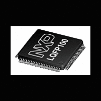
LPC2364HBD100 NXP Semiconductors, LPC2364HBD100 Datasheet - Page 14

LPC2364HBD100
Manufacturer Part Number
LPC2364HBD100
Description
LPC2364HBD100/LQFP100/TRAYBDP/
Manufacturer
NXP Semiconductors
Series
LPC2300r
Datasheet
1.LPC2364FBD100551.pdf
(59 pages)
Specifications of LPC2364HBD100
Core Processor
ARM7
Core Size
16/32-Bit
Speed
72MHz
Connectivity
CAN, Ethernet, I²C, Microwire, SPI, SSI, SSP, UART/USART, USB
Peripherals
Brown-out Detect/Reset, DMA, I²S, POR, PWM, WDT
Number Of I /o
70
Program Memory Size
128KB (128K x 8)
Program Memory Type
FLASH
Ram Size
34K x 8
Voltage - Supply (vcc/vdd)
3 V ~ 3.6 V
Data Converters
A/D 6x10b; D/A 1x10b
Oscillator Type
Internal
Operating Temperature
-40°C ~ 125°C
Package / Case
100-LQFP
Processor Series
LPC23
Core
ARM7TDMI-S
3rd Party Development Tools
MDK-ARM, RL-ARM, ULINK2, SAB-TFBGA100
Lead Free Status / RoHS Status
Lead free / RoHS Compliant
Eeprom Size
-
Lead Free Status / Rohs Status
Details
Available stocks
Company
Part Number
Manufacturer
Quantity
Price
Company:
Part Number:
LPC2364HBD100
Manufacturer:
NXP
Quantity:
479
Company:
Part Number:
LPC2364HBD100
Manufacturer:
NXP Semiconductors
Quantity:
10 000
Part Number:
LPC2364HBD100
Manufacturer:
NXP/恩智浦
Quantity:
20 000
Company:
Part Number:
LPC2364HBD100,551
Manufacturer:
NXP Semiconductors
Quantity:
10 000
Part Number:
LPC2364HBD100,551
Manufacturer:
NXP/恩智浦
Quantity:
20 000
NXP Semiconductors
Table 4.
LPC2364_65_66_67_68_6
Product data sheet
Symbol
P2[11]/EINT1/
MCIDAT1/
I2STX_CLK
P2[12]/EINT2/
MCIDAT2/
I2STX_WS
P2[13]/EINT3/
MCIDAT3/
I2STX_SDA
P3[0] to P3[31]
P3[25]/MAT0[0]/
PWM1[2]
P3[26]/MAT0[1]/
PWM1[3]
P4[0] to P4[31]
P4[28]/MAT2[0]/
TXD3
P4[29]/MAT2[1]/
RXD3
DBGEN
TDO
TDI
TMS
TRST
Pin description
Pin
52
51
50
27
26
82
85
-
1
2
3
4
[1]
[1]
[1]
[1]
[6]
[6]
[6]
[1]
[1]
[1]
[1]
…continued
Ball
H8
K10
J9
H3
K1
C7
E6
D4
A1
C3
B1
C2
[6]
[1]
[1]
[1]
[1]
[6]
[1]
[1]
[1]
[1]
[1]
[6]
Type
I/O
I
O
I/O
I/O
I
O
I/O
I/O
I
O
I/O
I/O
I/O
O
O
I/O
O
O
I/O
I/O
O
O
I/O
O
I
I
O
I
I
I
Description
P2[11] — General purpose digital input/output pin.
EINT1 — External interrupt 1 input.
MCIDAT1 — Data line for SD/MMC interface. (LPC2367/68 only)
I2STX_CLK — Transmit Clock. It is driven by the master and received by
the slave. Corresponds to the signal SCK in the I
P2[12] — General purpose digital input/output pin.
EINT2 — External interrupt 2 input.
MCIDAT2 — Data line for SD/MMC interface. (LPC2367/68 only)
I2STX_WS — Transmit Word Select. It is driven by the master and
received by the slave. Corresponds to the signal WS in the I
specification.
P2[13] — General purpose digital input/output pin.
EINT3 — External interrupt 3 input.
MCIDAT3 — Data line for SD/MMC interface. (LPC2367/68 only)
I2STX_SDA — Transmit data. It is driven by the transmitter and read by the
receiver. Corresponds to the signal SD in the I
Port 3: Port 3 is a 32-bit I/O port with individual direction controls for each
bit. The operation of Port 3 pins depends upon the pin function selected via
the pin connect block. Pins 0 through 24, and 27 through 31 of this port are
not available.
P3[25] — General purpose digital input/output pin.
MAT0[0] — Match output for Timer 0, channel 0.
PWM1[2] — Pulse Width Modulator 1, output 2.
P3[26] — General purpose digital input/output pin.
MAT0[1] — Match output for Timer 0, channel 1.
PWM1[3] — Pulse Width Modulator 1, output 3.
Port 4: Port 4 is a 32-bit I/O port with individual direction controls for each
bit. The operation of Port 4 pins depends upon the pin function selected via
the pin connect block. Pins 0 through 27, 30, and 31 of this port are not
available.
P4[28] — General purpose digital input/output pin.
MAT2[0] — Match output for Timer 2, channel 0.
TXD3 — Transmitter output for UART3.
P4[29] — General purpose digital input/output pin.
MAT2[1] — Match output for Timer 2, channel 1.
RXD3 — Receiver input for UART3.
DBGEN — JTAG interface control signal. Also used for boundary scanning.
Note: This pin is available in LPC2364FET100 and LPC2368FET100
devices only (TFBGA package).
TDO — Test Data out for JTAG interface.
TDI — Test Data in for JTAG interface.
TMS — Test Mode Select for JTAG interface.
TRST — Test Reset for JTAG interface.
Rev. 06 — 1 February 2010
LPC2364/65/66/67/68
Single-chip 16-bit/32-bit microcontrollers
2
S-bus specification.
2
S-bus specification.
© NXP B.V. 2010. All rights reserved.
2
S-bus
14 of 59


