FDS8962C Fairchild Semiconductor, FDS8962C Datasheet
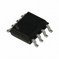
MOSFET N/P-CH DUAL 30V 8SOIC

FDS8962C

Manufacturer Part Number
FDS8962C
Description
MOSFET N/P-CH DUAL 30V 8SOIC
Manufacturer
Fairchild Semiconductor
Series
PowerTrench®r
Datasheet

Specifications of FDS8962C

Fet Type
N and P-Channel
Fet Feature
Logic Level Gate
Rds On (max) @ Id, Vgs
30 mOhm @ 7A, 10V
Drain To Source Voltage (vdss)
30V
Current - Continuous Drain (id) @ 25° C
7A, 5A
Vgs(th) (max) @ Id
3V @ 250µA
Gate Charge (qg) @ Vgs
26nC @ 10V
Input Capacitance (ciss) @ Vds
575pF @ 15V
Power - Max
900mW
Mounting Type
Surface Mount
Package / Case
8-SOIC (3.9mm Width)
Configuration
Dual Dual Drain
Transistor Polarity
N and P-Channel
Resistance Drain-source Rds (on)
0.03 Ohms / 0.052 Ohms
Forward Transconductance Gfs (max / Min)
25 S, 10 S
Drain-source Breakdown Voltage
+/- 30 V
Gate-source Breakdown Voltage
+/- 20 V
Continuous Drain Current
7 A, - 5 A
Power Dissipation
2 W
Maximum Operating Temperature
+ 150 C
Mounting Style
SMD/SMT
Minimum Operating Temperature
- 55 C
Lead Free Status / RoHS Status
Lead free / RoHS Compliant
Other names
FDS8962C

Available stocks

Company
Part Number
Manufacturer
Quantity
Price
Part Number:
FDS8962C
Manufacturer:
FSC
Quantity:
1 580
Part Number:
FDS8962C-NL
Manufacturer:
FAIRCHILD
Quantity:
12 639
©2005 Fairchild Semiconductor Corporation
FDS8962C Rev. A1
FDS8962C
Dual N & P-Channel PowerTrench
Features
■ Q1: N-Channel
■ Q2: P-Channel
■ Fast switching speed
■ High power and handling capability in a widely used surface
Absolute Maximum Ratings
Package Marking and Ordering Information
V
V
I
P
T
Thermal Characteristics
R
R
Symbol
D
J
DSS
GSS
D
θ JA
θ JC
mount package
, T
7.0A, 30V R
-5A, -30V R
Device Marking
STG
FDS8962C
Drain-Source Voltage
Gate-Source Voltage
Drain Current
Power Dissipation for Dual Operation
Power Dissipation for Single Operation
Operating and Storage Junction Temperature Range
Thermal Resistance, Junction-to-Ambient
Thermal Resistance, Junction-to-Case
R
R
DS(on)
DS(on)
DS(on)
DS(on)
SO-8
D1
= 0.030 Ω @ V
= 0.044 Ω @ V
= 0.052 Ω @ V
= 0.080 Ω @ V
D1
Pin 1
D2
– Continuous
– Pulsed
D2
Parameter
FDS8962C
Device
GS
GS
GS
GS
S1
= 10V
= 4.5V
= -10V
= -4.5V
G1
T
S2
A
= 25°C unless otherwise noted
G2
Reel Size
(Note 1a)
(Note 1a)
(Note 1b)
(Note 1a)
(Note 1c)
(Note 1)
13”
1
General Description
These dual N- and P-Channel enhancement mode power field
effect transistors are produced using Fairchild Semiconductor’s
advanced PowerTrench process that has been especially
tailored to minimize on-state ressitance and yet maintain
superior switching performance.
These devices are well suited for low voltage and battery
powered applications where low in-line power loss and fast
switching are required.
®
MOSFET
Q1
± 20
20
30
7
5
6
7
8
Tape width
-55 to +150
12mm
1.6
0.9
Q2
Q1
78
40
2
1
Q2
± 20
-20
-30
-5
4
3
2
1
www.fairchildsemi.com
Quantity
2500 units
June 2006
Units
° C/W
° C/W
° C
W
V
V
A

Related parts for FDS8962C

FDS8962C Summary of contents

Page 1

... R Thermal Resistance, Junction-to-Case θ JC Package Marking and Ordering Information Device Marking FDS8962C FDS8962C ©2005 Fairchild Semiconductor Corporation FDS8962C Rev. A1 ® General Description These dual N- and P-Channel enhancement mode power field = 10V effect transistors are produced using Fairchild Semiconductor’ 4.5V advanced PowerTrench process that has been especially ...

Page 2

... Turn-On Rise Time r t Turn-Off Delay Time d(off) t Turn-Off Fall Time f Q Total Gate Charge g Q Gate-Source Charge gs Q Gate-Drain Charge gd FDS8962C Rev 25°C unless otherwise noted A Test Conditions = 250 µ -250 µ 250 µ A, Referenced to 25 ° -250 µA, Referenced to 25 ° C ...

Page 3

... R is determined by the user's board design. θJC θCA a) 78°/W when mounted 0.5 in pad copper Scale letter size paper 2. Pulse Test: Pulse Width < 300µs, Duty Cycle < 2.0% FDS8962C Rev 25°C unless otherwise noted A Test Conditions 1.3 A (Note ...

Page 4

... JUNCTION TEMPERATURE (°C) J Figure 3. On-Resistance Variation with Temperature 125° 1 GATE TO SOURCE VOLTAGE (V) GS Figure 5. Transfer Characteristics. FDS8962C Rev. A1 2.2 3.5V 1 3.5V GS 1.4 3.0V 1 0.6 0 1.5 2 Figure 2. On-Resistance Variation with Drain Current and Gate Voltage. 0.08 0.07 0.06 0.05 0.04 0. 25° ...

Page 5

... Figure 7. Gate Charge Characteristics. 100 R LIMIT DS(ON 10s 10V GS SINGLE PULSE 0.1 R θ 135°C 25°C A 0.01 0 DRAIN-SOURCE VOLTAGE (V) DS Figure 9. Maximum Safe Operating Area. FDS8962C Rev. A1 800 V = 10V 20V DS 600 15V 400 200 C rss Figure 8. Capacitance Characteristics. 50 100µs 40 1ms 10ms 100ms ...

Page 6

... T , JUNCTION TEMPERATURE (°C) J Figure 13. On-Resistance Variation with Temperature - 1 GATE TO SOURCE VOLTAGE (V) GS Figure 15. Transfer Characteristics. FDS8962C Rev 1 -4.5V 1.6 -4.0V 1.4 1.2 -3.5V 1 -3.0V 0 Figure 12. On-Resistance Variation with Drain Current and Gate Voltage. 0.25 0.2 0.15 0 25°C A ...

Page 7

... A 0.01 0 DRAIN-SOURCE VOLTAGE (V) DS Figure 19. Maximum Safe Operating Area 0.5 0.2 0.1 0.1 0.05 0.02 0.01 0.01 SINGLE PULSE 0.001 0.0001 0.001 FDS8962C Rev. A1 800 V = -5V 700 DS -10V 600 -15V 500 400 300 200 100 C rss Figure 18. Capacitance Characteristics. ...

Page 8

... TRADEMARKS The following are registered and unregistered trademarks Fairchild Semiconductor owns or is authorized to use and is not intended exhaustive list of all such trademarks. ® ACEx™ FAST ActiveArray™ FASTr™ Bottomless™ FPS™ Build it Now™ FRFET™ CoolFET™ ...

Related keywords