FQA62N25C Fairchild Semiconductor, FQA62N25C Datasheet

MOSFET N-CH 250V 62A TO-3P

FQA62N25C

Manufacturer Part Number
FQA62N25C
Description
MOSFET N-CH 250V 62A TO-3P
Manufacturer
Fairchild Semiconductor
Series
QFET™r
Datasheet

Specifications of FQA62N25C

Fet Type
MOSFET N-Channel, Metal Oxide
Fet Feature
Standard
Rds On (max) @ Id, Vgs
35 mOhm @ 31A, 10V
Drain To Source Voltage (vdss)
250V
Current - Continuous Drain (id) @ 25° C
62A
Vgs(th) (max) @ Id
4V @ 250µA
Gate Charge (qg) @ Vgs
130nC @ 10V
Input Capacitance (ciss) @ Vds
6280pF @ 25V
Power - Max
298W
Mounting Type
Through Hole
Package / Case
TO-3PN-3
Configuration
Single
Transistor Polarity
N-Channel
Resistance Drain-source Rds (on)
0.035 Ohm @ 10 V
Forward Transconductance Gfs (max / Min)
55 S
Drain-source Breakdown Voltage
250 V
Gate-source Breakdown Voltage
+/- 30 V
Continuous Drain Current
62 A
Power Dissipation
298000 mW
Maximum Operating Temperature
+ 150 C
Mounting Style
Through Hole
Minimum Operating Temperature
- 55 C
Continuous Drain Current Id
62A
Drain Source Voltage Vds
250V
On Resistance Rds(on)
35mohm
Rds(on) Test Voltage Vgs
10V
Threshold Voltage Vgs Typ
4V
Rohs Compliant
Yes
Lead Free Status / RoHS Status
Lead free / RoHS Compliant

Available stocks

Company
Part Number
Manufacturer
Quantity
Price
Part Number:
FQA62N25C
Manufacturer:
FAIRCHILD
Quantity:
12 500
Part Number:
FQA62N25C
Manufacturer:
FSC
Quantity:
86 755
Part Number:
FQA62N25C
Manufacturer:
FAIRCHILD
Quantity:
2 644
©2004 Fairchild Semiconductor Corporation
FQA62N25C
250V N-Channel MOSFET
General Description
These N-Channel enhancement mode power field effect
transistors are produced using Fairchild’s proprietary,
planar, DMOS technology.
This advanced technology has been especially tailored to
minimize on-state resistance, provide superior switching
performance, and withstand high energy pulse in the
avalanche and commutation mode. These devices are well
suited for high efficiency switching DC/DC converters and
switch mode power supplies.
Absolute Maximum Ratings
Thermal Characteristics
V
I
I
V
E
I
E
dv/dt
P
T
T
R
R
R
D
DM
AR
J
L
DSS
GSS
AS
AR
D
Symbol
Symbol
θJC
θCS
θJA
, T
STG
Drain-Source Voltage
Drain Current
Drain Current
Gate-Source Voltage
Single Pulsed Avalanche Energy
Avalanche Current
Repetitive Avalanche Energy
Peak Diode Recovery dv/dt
Power Dissipation (T
Operating and Storage Temperature Range
Maximum lead temperature for soldering purposes,
1/8" from case for 5 seconds
Thermal Resistance, Junction-to-Case
Thermal Resistance, Case-to-Sink
Thermal Resistance, Junction-to-Ambient
G
D
S
- Continuous (T
- Continuous (T
- Pulsed
- Derate above 25°C
C
Parameter
= 25°C)
Parameter
TO-3PN
FQA Series
T
C
C
C
= 25°C unless otherwise noted
= 25°C)
= 100°C)
(Note 1)
(Note 2)
(Note 1)
(Note 1)
(Note 3)
Features
• 62A, 250V, R
• Low gate charge ( typical 100 nC)
• Low Crss ( typical 63.5 pF)
• Fast switching
• 100% avalanche tested
• Improved dv/dt capability
G
DS(on)
0.24
Typ
--
--
FQA62N25C
-55 to +150
= 0.035Ω @V
D
S
2300
29.8
2.38
± 30
250
248
298
300
5.5
62
39
62
Max
0.42
40
--
QFET
GS
= 10 V
Units
W/°C
Units
Rev. A, March 2004
°C/W
°C/W
°C/W
V/ns
mJ
mJ
°C
°C
W
V
A
A
A
V
A
®

Related parts for FQA62N25C

FQA62N25C Summary of contents

Page 1

... C Parameter QFET = 0.035Ω DS(on ● ● ◀ ◀ ▲ ▲ G ● ● ● ● S FQA62N25C Units 250 62 39 248 ± 30 2300 mJ 62 29.8 mJ 5.5 V/ns 298 2.38 W/°C -55 to +150 °C 300 Typ Max Units -- 0.42 ° ...

Page 2

... G ≤ 62A, di/dt ≤ 300A/µs, V ≤ Starting DSS, 4. Pulse Test : Pulse width ≤ 300µs, Duty cycle ≤ Essentially independent of operating temperature ©2004 Fairchild Semiconductor Corporation T = 25°C unless otherwise noted C Test Conditions = 250 µ 250 µA, Referenced to 25°C ...

Page 3

... Figure 3. On-Resistance Variation vs Drain Current and Gate Voltage 10000 8000 C iss 6000 C oss 4000 2000 ※ Notes : rss MHz Drain-Source Voltage [V] DS Figure 5. Capacitance Characteristics ©2004 Fairchild Semiconductor Corporation Notes : ※ 1. 250µ s Pulse Test ℃ Figure 2. Transfer Characteristics 20V GS ※ ...

Page 4

... DC Notes : ※ 150 Single Pulse - Drain-Source Voltage [V] DS Figure 9. Maximum Safe Operating Area ©2004 Fairchild Semiconductor Corporation (Continued) 3.0 2.5 2.0 1.5 1.0 Notes : ※ 0 250 µA D 0.0 100 150 200 -100 o C] Figure 8. On-Resistance Variation µ s 100 µ Figure 10. Maximum Drain Current ※ ...

Page 5

... Resistive Switching Test Circuit & Waveforms 10V 10V Unclamped Inductive Switching Test Circuit & Waveforms 10V 10V ©2004 Fairchild Semiconductor Corporation Gate Charge Test Circuit & Waveform Same Type Same Type as DUT as DUT 10V 10V DUT DUT DUT DUT ...

Page 6

... Peak Diode Recovery dv/dt Test Circuit & Waveforms Driver ) ( Driver ) DUT ) ( DUT ) DUT ) ( DUT ) ©2004 Fairchild Semiconductor Corporation + + DUT DUT Driver Driver Same Type Same Type as DUT as DUT • dv/dt controlled by R • dv/dt controlled by R • I • I controlled by pulse period ...

Page 7

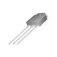
... Mechanical Dimensions ©2004 Fairchild Semiconductor Corporation TO-3PN Dimensions in Millimeters Rev. A, March 2004 ...

Page 8

... TRADEMARKS The following are registered and unregistered trademarks Fairchild Semiconductor owns or is authorized to use and is not intended exhaustive list of all such trademarks. ACEx™ FACT Quiet series™ ® ActiveArray™ FAST Bottomless™ FASTr™ CoolFET™ FPS™ CROSSVOLT™ ...

Related keywords