BLF245B,112 NXP Semiconductors, BLF245B,112 Datasheet - Page 3
BLF245B,112
Manufacturer Part Number
BLF245B,112
Description
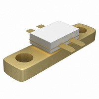
TRANSISTOR RF DMOS SOT279A
Manufacturer
NXP Semiconductors
Datasheet
1.BLF245B112.pdf
(14 pages)
Specifications of BLF245B,112
Package / Case
SOT-279A
Transistor Type
2 N-Channel (Dual)
Frequency
175MHz
Gain
18dB
Voltage - Rated
65V
Current Rating
4.5A
Current - Test
25mA
Voltage - Test
28V
Power - Output
30W
Minimum Operating Temperature
- 65 C
Mounting Style
SMD/SMT
Resistance Drain-source Rds (on)
1.5 Ohm @ 10 V
Transistor Polarity
N-Channel
Configuration
Dual Common Source
Drain-source Breakdown Voltage
65 V
Gate-source Breakdown Voltage
+/- 20 V
Continuous Drain Current
4.5 A
Power Dissipation
75000 mW
Maximum Operating Temperature
+ 200 C
Application
VHF
Channel Type
N
Channel Mode
Enhancement
Drain Source Voltage (max)
65V
Output Power (max)
30W
Power Gain (typ)@vds
18@28VdB
Frequency (max)
175MHz
Package Type
CDFM
Pin Count
5
Forward Transconductance (typ)
0.85S
Drain Source Resistance (max)
1500@10Vmohm
Input Capacitance (typ)@vds
60@28VpF
Output Capacitance (typ)@vds
40@28VpF
Reverse Capacitance (typ)
4.5@28VpF
Operating Temp Range
-65C to 200C
Drain Efficiency (typ)
65%
Mounting
Screw
Mode Of Operation
CW Class-B
Number Of Elements
2
Power Dissipation (max)
75000mW
Vswr (max)
50
Screening Level
Military
Lead Free Status / RoHS Status
Lead free / RoHS Compliant
Noise Figure
-
Lead Free Status / Rohs Status
Lead free / RoHS Compliant
Other names
568-2388
934003520112
BLF245B
BLF245B
934003520112
BLF245B
BLF245B


Philips Semiconductors
LIMITING VALUES
In accordance with the Absolute Maximum System (IEC 60134).
THERMAL CHARACTERISTICS
2003 Aug 04
Per transistor section unless otherwise specified
V
I
P
T
T
R
R
handbook, halfpage
SYMBOL
D
SYMBOL
V
stg
j
DS
tot
th j-mb
th mb-h
VHF push-pull power MOS transistor
(1) Current in this area may be limited by R
(2) T
Total device; both sections equally loaded.
GS
10
10
(A)
I D
10
mb
1
2
1
1
= 25 C.
drain-source voltage
gate-source voltage
DC drain current
total power dissipation
storage temperature
junction temperature
(1)
thermal resistance from
junction to mounting base
thermal resistance from
mounting base to heatsink
PARAMETER
Fig.2 DC SOAR.
PARAMETER
10
V DS (V)
DSon
T
mb
(2)
.
total device; both sections equally loaded
total device; both sections equally loaded
MRA922
25 C; total device; both sections equally loaded
10
2
CONDITIONS
3
CONDITIONS
handbook, halfpage
(1) Continuous operation.
(2) Short-time operation during mismatch.
Total device; both sections equally loaded.
P tot
(W)
120
80
40
0
0
Fig.3 Power derating curves.
40
(1)
(2)
80
MIN.
65
VALUE
Product specification
2.3
0.3
120
T h (
BLF245B
65
20
4.5
75
+150
200
MAX.
MRA929
o
C)
160
UNIT
K/W
K/W
V
V
A
W
UNIT
C
C
Related parts for BLF245B,112
Image
Part Number
Description
Manufacturer
Datasheet
Request
R

Part Number:
Description:
Dual push-pull silicon N-channel enhancement mode vertical D-MOS transistor designed for large signal amplifier applications in the VHF frequency range
Manufacturer:
NXP Semiconductors
Datasheet:

Part Number:
Description:
Silicon N-channel enhancement mode vertical D-MOS transistor designed for large signal amplifier applications in the VHF frequency range
Manufacturer:
NXP Semiconductors
Datasheet:

Part Number:
Description:
TRANSISTOR RF DMOS SOT123A
Manufacturer:
NXP Semiconductors
Datasheet:

Part Number:
Description:
NXP Semiconductors designed the LPC2420/2460 microcontroller around a 16-bit/32-bitARM7TDMI-S CPU core with real-time debug interfaces that include both JTAG andembedded trace
Manufacturer:
NXP Semiconductors
Datasheet:

Part Number:
Description:
NXP Semiconductors designed the LPC2458 microcontroller around a 16-bit/32-bitARM7TDMI-S CPU core with real-time debug interfaces that include both JTAG andembedded trace
Manufacturer:
NXP Semiconductors
Datasheet:
Part Number:
Description:
NXP Semiconductors designed the LPC2468 microcontroller around a 16-bit/32-bitARM7TDMI-S CPU core with real-time debug interfaces that include both JTAG andembedded trace
Manufacturer:
NXP Semiconductors
Datasheet:
Part Number:
Description:
NXP Semiconductors designed the LPC2470 microcontroller, powered by theARM7TDMI-S core, to be a highly integrated microcontroller for a wide range ofapplications that require advanced communications and high quality graphic displays
Manufacturer:
NXP Semiconductors
Datasheet:
Part Number:
Description:
NXP Semiconductors designed the LPC2478 microcontroller, powered by theARM7TDMI-S core, to be a highly integrated microcontroller for a wide range ofapplications that require advanced communications and high quality graphic displays
Manufacturer:
NXP Semiconductors
Datasheet:
Part Number:
Description:
The Philips Semiconductors XA (eXtended Architecture) family of 16-bit single-chip microcontrollers is powerful enough to easily handle the requirements of high performance embedded applications, yet inexpensive enough to compete in the market for hi
Manufacturer:
NXP Semiconductors
Datasheet:
Part Number:
Description:
The XA-S3 device is a member of Philips Semiconductors? XA(eXtended Architecture) family of high performance 16-bitsingle-chip microcontrollers
Manufacturer:
NXP Semiconductors
Datasheet:

Part Number:
Description:
The NXP BlueStreak LH75401/LH75411 family consists of two low-cost 16/32-bit System-on-Chip (SoC) devices
Manufacturer:
NXP Semiconductors
Datasheet:
Part Number:
Description:
The NXP LPC3130/3131 combine an 180 MHz ARM926EJ-S CPU core, high-speed USB2
Manufacturer:
NXP Semiconductors
Datasheet:
Part Number:
Description:
The NXP LPC3141 combine a 270 MHz ARM926EJ-S CPU core, High-speed USB 2
Manufacturer:
NXP Semiconductors
Part Number:
Description:
The NXP LPC3143 combine a 270 MHz ARM926EJ-S CPU core, High-speed USB 2
Manufacturer:
NXP Semiconductors